PGA400-Q1
SLDS186 –MARCH 2012
www.ti.com
5.17 Diagnostics
PARAMETER
TEST CONDITIONS
MIN
TYP
500
40
MAX
UNIT
ms
8051 Software watchdog
Main clock normal operation range
35
45
MHz
Sensor supply over voltage
threshold
VBRG_OV
VBRG_UV
3.55
3.65
3.0
3.75
V
V
Sensor supply under voltage
threshold
2.9
3.11
AVDD OV threshold
AVDD UV threshold
3.75
2.72
3.95
3.1
V
V
Output overvoltage threshold for
gain stage 1 and 2
SensorOV
SensorUV
f_capHigh
f_capLow
2.4
0.7
1.5
30
2.5
.85
2.6
1.0
2.5
50
V
V
Output undervoltage threshold for
gain stage 1 and 2
Capacitive sensor interface clock
high frequency fault threshold
MHz
kHz
V
Capacitive sensor interface clock
low frequency fault threshold
EEPROM CHG PUMP overvoltage
threshold
14.65
EEPROM CHG PUMP undervoltage
threshold
11.45
0.545
V
DAC loop back voltage gain
0.537
0.557
2
V/V
µA
Open wire leakage current 1 - open
VDD with pull-up on VOUT1
Open wire leakage current 2 - open
GND with pull-down on VOUT1
20
µA
6 FUNCTIONAL DESCRIPTIONS
In this section, individual blocks in the Section 2 are described in more detail.
6.1 Overvoltage / Reverse Voltage Protection Block
The PGA400-Q1 includes an Overvoltage and Reverse Voltage Protection block. This block protects the
device from overvoltage and reverse-battery conditions on the external power supply. In this block, a
control circuit monitors the input supply line for reverse-battery and overvoltage fault conditions protects
the device if these voltage conditions occur on the external power supply.
6.2 Linear Regulators and Bandgap + Current Blocks
The PGA400-Q1 contains two precision low-drift bandgap supply voltage references for other blocks of the
device. One bandgap provides the reference voltage for internal linear regulators that supply AVDD and
DVDD. The other bandgap reference provides the voltage reference for the all the other internal circuitry,
including sensor supply regulators, sensor offset compensation, etc.
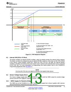
The PGA400-Q1 has two main linear regulators: AVDD Regulator and DVDD Regulator. The AVDD
regulator provides the 3.3 V voltage source for internal analog circuitry while the DVDD regulator provides
the 3.3 V regulated voltage for the digital circuitry. The user needs to connect bypass capacitors of 100nF
on both the AVDD and DVDD pins of the device.
Figure 6-1 shows the Power-On Reset sequence for AVDD and DVDD with respect to the voltage applied
to the VDD pin.
12
FUNCTIONAL DESCRIPTIONS
Copyright © 2012, Texas Instruments Incorporated
Submit Documentation Feedback
Product Folder Link(s): PGA400-Q1

 TI [ TEXAS INSTRUMENTS ]