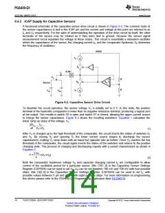
PGA400-Q1
SLDS186 –MARCH 2012
www.ti.com
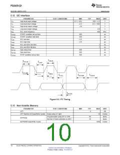
5.12 I2C Interface
PARAMETER
TEST CONDITIONS
MIN
0.7 × VDD
–0.3
TYP
MAX
VDD + 0.3
0.3 × VDD
UNIT
V
VIH
High-level input voltage
Low-level input voltage
High-level output voltage
Low-level output voltage
SCL clock frequency
START condition set-up time
START condition hold time
SCL low time
VIL
V
VOH
4.0
V
VOL
0.8
V
fSCL
400
KHz
ns
ns
µs
µs
ns
ns
ns
ns
ns
tSTASU
tSTAHD
tLOW
tHIGH
tRISE
tFALL
tDATSU
tDATHD
tSTOSU
500
500
1.25
1.25
SCL high time
SCL and SDA rise time
SCL and SDA fall time
Data setup time
7
7
500
500
500
Data hold time
STOP condition set-up time
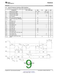
Figure 5-2. I2C Timing
5.13 Non-Volatile Memory
PARAMETER
TEST CONDITIONS
MIN
TYP
MAX
UNIT
KB
OTP
8
OTP Number of Erase/Write Cycles Erase using UV light
10
Cycles
Bytes
Bytes
Cycles
Programmable using SPI or OWI
Number of bytes writeable by 8051
89
16
EEPROM
EEPROM Erase/Write Cycles
1000
10
ELECTRICAL CHARACTERISTICS
Copyright © 2012, Texas Instruments Incorporated
Submit Documentation Feedback
Product Folder Link(s): PGA400-Q1

 TI [ TEXAS INSTRUMENTS ]