PCM9211
SBAS495 –JUNE 2010
www.ti.com
STATE of
SYNCHRONIZATION
synchronous
Asynchronous
synchronous
within 2 /f
S
t
ADCDL3Y
32/f
S
Undefined data
ADC
DOUT
Normal
ZERO
Normal
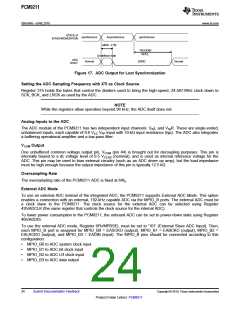
Figure 17. ADC Output for Lost Synchronization
Setting the ADC Sampling Frequency with XTI as Clock Source
Register 31h holds the bytes that control the dividers used to bring the high-speed, 24.567-MHz clock down to
SCK, BCK, and LRCK as used by the ADC.
NOTE
While the registers allow operation beyond 96 kHz, the ADC itself does not.
Analog Inputs to the ADC
The ADC module of the PCM9211 has two independent input channels: VINL and VINR. These are single-ended,
unbalanced inputs, each capable of 0.6 VCC VPP input with 10-kΩ input resistance (typ). The ADC also integrates
a buffering operational amplifier and a low-pass filter.
VCOM Output
One unbuffered common voltage output pin, VCOM (pin 44) is brought out for decoupling purposes. This pin is
internally biased to a dc voltage level of 0.5 VCCAD (nominal), and is used as internal reference voltage for the
ADC. This pin may be used to bias external circuitry (such as an ADC driver op amp), but the load impedance
must be high enough because the output impedance of this pin is typically 12.5 kΩ.
Oversampling Rate
The oversampling rate of the PCM9211 ADC is fixed at 64fS.
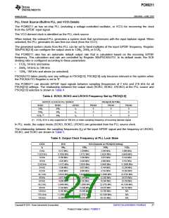
External ADC Mode
To use an external ADC instead of the integrated ADC, the PCM9211 supports External ADC Mode. This option
enables a connection with an external, 192-kHz capable ADC via the MPIO_B ports. The external ADC must be
a clock slave to the PCM9211. The clock source for the external ADC can be selected using Register
42h/ADCLK (the same register that controls the clock source for the internal ADC).
To lower power consumption in the PCM9211, the onboard ADC can be set to power-down state using Register
40h/ADDIS.
To use the external ADC mode, Register 6Fh/MPBSEL must be set to '101' (External Slave ADC Input). Then,
each MPIO_B port is assigned for MPIO_B0 = EASCKO (output), MPIO_B1 = EABCKO (output), MPIO_B2 =
EALRCKO (output), and MPIO_B3 = EADIN (input). The MPIO_B pins should be connected according to this
configuration:
•
•
•
•
MPIO_B0 to ADC system clock input
MPIO_B1 to ADC bit clock input
MPIO_B2 to ADC LR clock input
MPIO_B3 to ADC data output
24
Submit Documentation Feedback
Copyright © 2010, Texas Instruments Incorporated
Product Folder Link(s): PCM9211

 TI [ TEXAS INSTRUMENTS ]