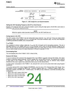
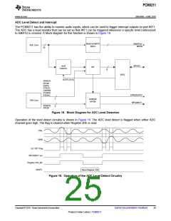
PCM9211
SBAS495 –JUNE 2010
www.ti.com
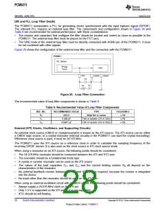
DIR and PLL Loop Filter Details
The PCM9211 incorporates a PLL for generating clocks synchronized with the input biphase signal (S/PDIF).
The onboard PLL requires an external loop filter. The components and configuration shown in Figure 20 and
Table 6 are recommended for optimal performance, with these considerations:
•
The resistor and capacitors that configure the filter should be located and routed as close as possible to the
PCM9211. The external loop filter must be placed on the FILT pins.
•
The GND node of the external loop filter must be directly connected with AGND pin of the PCM9211; it must
be not combined with other signals.
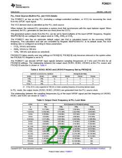
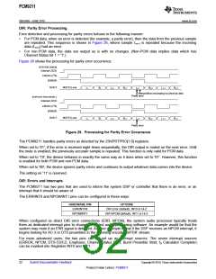
Figure 20 shows the configuration of the external loop filter and the connection with the PCM9211.
PCM9211
PLL Section
Charge
VCO
Pump
FILT
C2
AGND
DGND
C1
R1
Figure 20. Loop Filter Connection
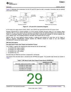
The recommended value of loop filter components is shown in Table 6.
Table 6. Recommended Value of Loop Filter Components
REF. NO.
RECOMMENDED VALUE
680 Ω
TYPE
TOLERANCE
≤ 5%
R1
C1
C2
Metal film or carbon
0.068 µF
Film or ceramic (CH or C0G)
Film or ceramic (CH or C0G)
≤ 5%
0.0047 µF
≤ 5%
External (XTI) Clocks, Oscillators, and Supporting Circuitry
An external clock source (CMOS or crystal/resonator) is known as the XTI source. The XTI source can be either
a CMOS logic source, or a crystal resonator (internal circuitry in the PCM9211 can start the crystal resonating).
Whichever clock source is used, it must be 24.576 MHz.
The PCM9211 uses the XTI source as a reference clock in order to calculate the sampling frequency of the
incoming S/PDIF stream. It is also used as the clock source in XTI clock source mode.
When using a resonator as an XTI source, the following points should be considered:
•
•
•
•
The 24.576-MHz resonator should be connected between the XTI and XTO pins
The resonator should be a fundamental mode type
A crystal or ceramic resonator can be used as the XTI source
The values of the load capacitors CL1 and CL2 and the current limiting resistor Rd all depend on the
characteristics of the resonator
•
No external feedback resistor between the XTI and XTO pins is required, because the resistor is integrated
into the device
•
No loads other than the resonator should be used on the XTO pin
When using an external oscillation circuit with a CMOS output, the following points should be considered:
•
•
•
Always supply a 24.576-MHz clock on the XTI pin
Only 3.3 V is supported on the XTI pin; 5 V is not supported
XTO should be left floating
28
Submit Documentation Feedback
Copyright © 2010, Texas Instruments Incorporated
Product Folder Link(s): PCM9211

 TI [ TEXAS INSTRUMENTS ]