PCM9211
www.ti.com
SBAS495 –JUNE 2010
Additional ADC Functions
The onboard ADC has some additional functions. Control of these functions is done using several registers
(Register 40h through Register 49h).
Each ADC channel has a digital attenuator function. The level of attenuation can be set from 20 dB to –100 dB in
0.5-dB steps, and also set to infinite attenuation (mute). By default, the digital gain/attenuation is moved 0.5-dB
steps closer from its current level to its new setting only when the sampled output crosses zero (zero crossing).
Changing gain or attenuation at zero crossing points in the audio minimizes zipper noise.
If zero crossing is disabled, then the gain steps ±0.5 dB towards its target every 8/fS. Zero crossing detection is
modified using the ADZCDD register. If zero crossing is not detected for 512/fS (for example, if there is a
significant dc bias on the signal), then the level change is done on every samples (1/fS) until zero crossing is
detected again.
If updated volume change instructions are received during a volume change, they will be ignored until the current
change is complete.
The attenuation level for each channel can be set individually using the following formula:
Attenuation Level (dB) = 0.5 ● (AT1x[7:0]DEC – 215), where AT1x[7:0]DEC = 0 through 255
For ADATTL[7:0]DEC = 0 through 14, attenuation is set to infinite attenuation (mute).
For ADATTR[7:0]DEC = 0 through 14, attenuation is set to infinite attenuation (mute).
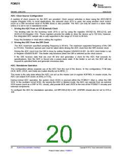
ADC: Power Down and Power Up
If synchronization is maintained among SCKI, BCK, and LRCK, the DOUT from the ADC is enabled and a
fade-in begins tADCDLY1 = 2048/fS after the internal reset is released. DOUT then starts to output data
corresponding to VINL and VINR after tADCDLY2 = 1936/fS from the start of fade-in. If synchronization is not
maintained, the internal reset is not released, and the ADC is held in reset. After resynchronization, the ADC
begins its fade-in operation after internal initialization and an initial delay. During fade-in (tADCDLY1 + tADCDLY2) and
fade-out (tADCDLY2), SCKI, BCK, and LRCK must be provided. Figure 14 illustrates the ADC output sequence at
power up and power down.
SCK
BCK
Synchronous Clocks
Synchronous Clocks
LRCK
ADDIS
2048/f min
S
1024 SCKIx
Internal
Reset
Normal Operation
power down
Normal Operation
tADCDLY2
t
ADCDLY2
tADCDLY1
2048/fS
1936/fS
1936/fS
DOUT
ZERO
Fade Out
Fade In
Figure 14. ADC Output at Power Up and Power Down
Copyright © 2010, Texas Instruments Incorporated
Submit Documentation Feedback
21
Product Folder Link(s): PCM9211

 TI [ TEXAS INSTRUMENTS ]