PCM9211
www.ti.com
SBAS495 –JUNE 2010
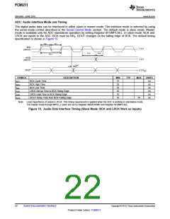
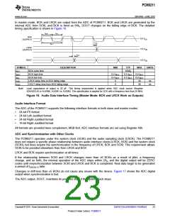
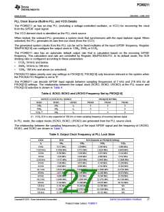
In master mode, BCK and LRCK are output from the ADC of PCM9211. BCK and LRCK are generated by the
internal ADC from SCKI, and BCK is fixed as 64fS. DOUT changes on the falling edge of BCK. The detailed
timing specification is shown in Figure 16.
tBCH
tBC L
BCK
(OUTPUT)
0.5 VDD
t LRD
tBC Y
LRCK
(OUTPUT)
0.5 VDD
tDOD
0.5 VDD
DOUT
SYMBOL
DESCRIPTION
MIN
TYP
MAX
UNITS
tBCY
tBCH
tBCL
tLRD
tDOD
BCK cycle time
BCK high time
BCK low time
1/64fS
0.4 tBCY
0.5 tBCY
0.5 tBCY
0.6 tBCY
0.6 tBCY
30
0.4 tBCY
LRCK delay time to BCK falling edge
DOUT delay time from BCK falling edge
0
0
ns
ns
30
Note: Load capacitance of output is 20 pF. This timing requirement is applied when ADC clock source (Register
42h/ADCLK) is AUXIN0, AUXIN1 or AUXIN2. This specification is applied for SCK with a frequency less than 25 MHz.
Figure 16. Audio Data Interface Timing (Master Mode: BCK and LRCK Work as Outputs)
Audio Interface Format
The ADC of the PCM9211 supports the following interface formats in both slave and master modes:
•
•
•
•
24-bit I2S format
24-bit Left-Justified format
24-bit Right-Justified format
16-bit Right-Justified format
All formats are provided twos complement, MSB first. ADC interface formats are set using Register 48h.
ADC and Synchronization with Other Clocks
The PCM9211 operates under the system clock (SCKI) and the audio sampling clock (LRCK). The PCM9211
does not require a specific phase relationship between audio interface clocks (LRCK, BCK) and the system clock
(SCKI), but does require the synchronization in the frequency of LRCK, BCK and SCKI. This requirement allows
SCKI to be provided elsewhere than from LRCK and BCK.
LRCK and BCK require synchronization at all times.
If the relationship between SCKI and LRCK changes more than ±6 BCKs as a result of jitter, a frequency
change, and so forth, the internal operation of the ADC stops within 2/fS, and the digital output will be ZERO
codes until resynchronization between SCKI and LRCK and BCK is completed. Real data begin to be generated
a period of tADCDLY3 later.
Changes or drift less than ±5 BCKs do not cause any issues with the device. Figure 17 shows the ADC digital
output when synchronization is lost.
The ADC output, DOUT, maintains its previous state if the system clock stops.
Copyright © 2010, Texas Instruments Incorporated
Submit Documentation Feedback
23
Product Folder Link(s): PCM9211

 TI [ TEXAS INSTRUMENTS ]