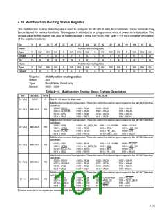
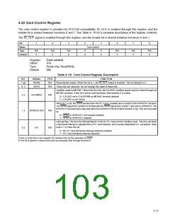
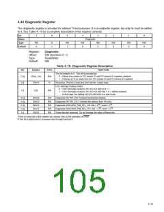
4.40 Diagnostic Register
The diagnostic register is provided for internal TI test purposes. It is a read/write register, but only 0s must be written
to it. See Table 4−18 for a complete description of the register contents.
Bit
7
6
5
4
3
2
1
0
Name
Type
Default
Diagnostic
RW
0
R
1
RW
1
RW
0
RW
0
RW
0
RW
0
RW
0
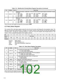
Register:
Offset:
Type:
Diagnostic
93h (functions 0, 1)
Read/Write
60h
Default:
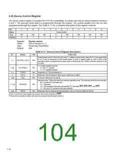
Table 4−18. Diagnostic Register Description
FUNCTION
BIT
7 ‡§
6 ‡
SIGNAL
TRUE_VAL
RSVD
TYPE
RW
R
This bit defaults to 0. This bit is encoded as:
0 = Reads true values in PCI vendor ID and PCI device ID registers (default)
1 = Returns all 1s to reads from the PCI vendor ID and PCI device ID registers
Reserved. This bit is read-only and returns 1 when read.
CSC interrupt routing control
0 = CSC interrupts routed to PCI if ExCA 803 bit 4 = 1
1 = CSC interrupts routed to PCI if ExCA 805 bits 7−4 = 0000b (default).
In this case, the setting of ExCA 803 bit 4 is a don’t care.
5 ‡
CSC
RW
4 ‡§
3 ‡§
2 ‡§
1 ‡§
0 ‡
DIAG4
DIAG3
DIAG2
DIAG1
RSVD
RW
RW
RW
RW
RW
Diagnostic RETRY_DIS. Delayed transaction disable.
Diagnostic RETRY_EXT. Extends the latency from 16 to 64.
10
15
.
Diagnostic DISCARD_TIM_SEL_CB. Set = 2 , reset = 2
10
15
.
Diagnostic DISCARD_TIM_SEL_PCI. Set = 2 , reset = 2
These bits are reserved. Do not change the value of these bits.
‡
§
One or more bits in this register are cleared only by the assertion of GRST.
This bit is global and is accessed only through function 0.
4−29

 TI [ TEXAS INSTRUMENTS ]