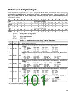
4.36 Multifunction Routing Status Register
The multifunction routing status register is used to configure the MFUNC6−MFUNC0 terminals. These terminals may
be configured for various functions. This register is intended to be programmed once at power-on initialization. The
default value for this register can also be loaded through a serial EEPROM. See Table 4−14 for a complete description
of the register contents.
Bit
31
30
29
28
27
26
25
24
23
22
21
20
19
18
17
16
Name
Type
Default
Multifunction routing status
R
0
RW
0
RW
0
RW
0
R
0
RW
0
RW
0
RW
0
R
0
RW
0
RW
0
RW
0
R
0
RW
0
RW
0
RW
0
Bit
15
14
13
12
11
10
9
8
7
6
5
4
3
2
1
0
Name
Type
Default
Multifunction routing status
R
0
RW
0
RW
0
RW
1
R
0
RW
0
RW
0
RW
0
R
0
RW
0
RW
0
RW
0
R
0
RW
0
RW
0
RW
0
Register:
Offset:
Type:
Multifunction routing status
8Ch
Read/Write, Read-only
0000 1000h
Default:
Table 4−14. Multifunction Routing Status Register Description
BIT
SIGNAL
TYPE
FUNCTION
31−28 ‡
RSVD
R
Bits 31−28 return 0s when read.
Multifunction terminal 6 configuration. These bits control the internal signal mapped to the MFUNC6 terminal
as follows:
0000 = RSVD
0001 = CLKRUN
0010 = IRQ2
0011 = IRQ3
0100 = IRQ4
0101 = IRQ5
0110 = IRQ6
0111 = IRQ7
1000 = IRQ8
1001 = IRQ9
1010 = IRQ10
1011 = IRQ11
1100 = IRQ12
1101 = IRQ13
1110 = IRQ14
1111 = IRQ15
27−24 ‡
23−20 ‡
MFUNC6
MFUNC5
RW
Multifunction terminal 5 configuration. These bits control the internal signal mapped to the MFUNC5 terminal
as follows:
0000 = GPI4
0001 = GPO4
0010 = PCGNT
0011 = IRQ3
0100 = SC_DBG_RX 1000 = CAUDPWM
1100 = LEDA1
1101 = LED_SKT
1110 = GPE
RW
RW
0101 = IRQ5
0110 = RSVD
0111 = RSVD
1001 = IRQ9
1010 = FM_LED
1011 = OHCI_LED
1111 = IRQ15
Multifunction terminal 4 configuration. These bits control the internal signal mapped to the MFUNC4 terminal
as follows:
0000 = GPI3
0100 = IRQ4
0101 = SC_DBG_TX 1001 = IRQ9
0110 = RSVD
0111 = RSVD
1000 = CAUDPWM
1100 = RI_OUT
1101 = LED_SKT
1110 = GPE
19−16 ‡
MFUNC4
0001 = GPO3
0010 = LOCK PCI
0011 = IRQ3
1010 = INTD
1011 = FM_LED
1111 = IRQ15
Multifunction terminal 3 configuration. These bits control the internal signal mapped to the MFUNC3 terminal
as follows:
0000 = RSVD
0001 = IRQSER
0010 = IRQ2
0011 = IRQ3
0100 = IRQ4
0101 = IRQ5
0110 = IRQ6
0111 = IRQ7
1000 = IRQ8
1001 = IRQ9
1010 = IRQ10
1011 = IRQ11
1100 = IRQ12
1101 = IRQ13
1110 = IRQ14
1111 = IRQ15
15−12 ‡
11−8 ‡
MFUNC3
MFUNC2
RW
RW
Multifunction terminal 2 configuration. These bits control the internal signal mapped to the MFUNC2 terminal
as follows:
0000 = GPI2
0001 = GPO2
0010 = PCREQ
0011 = IRQ3
0100 = IRQ4
0101 = IRQ5
0110 = RSVD
0111 = RSVD
1000 = CAUDPWM
1001 = FM_LED
1010 = IRQ10
1100 = RI_OUT
1101 = TEST_MUX
1110 = GPE
1011 = INTC
1111 = IRQ7
‡
One or more bits in this register are cleared only by the assertion of GRST.
4−25

 TI [ TEXAS INSTRUMENTS ]