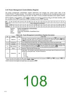
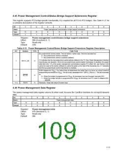
4.45 Power Management Control/Status Bridge Support Extensions Register
This register supports PCI bridge-specific functionality. It is required for all PCI-to-PCI bridges. See Table 4−21 for
a complete description of the register contents.
Bit
7
6
5
4
3
2
1
0
Name
Type
Default
Power management control/status bridge support extensions
R
1
R
1
R
0
R
0
R
0
R
0
R
0
R
0
Register:
Offset:
Type:
Power management control/status bridge support extensions
A6h (Functions 0, 1)
Read-only
Default:
C0h
Table 4−21. Power Management Control/Status Bridge Support Extensions Register Description
BIT
SIGNAL
TYPE
FUNCTION
Bus power/clock control enable. This bit returns 1 when read. This bit is encoded as:
0 = Bus power/clock control is disabled.
1 = Bus power/clock control is enabled (default).
A 0 indicates that the bus power/clock control policies defined in the PCI Bus Power Management Interface
Specification are disabled. When the bus power/clock control enable mechanism is disabled, the power
state field (bits 1−0) of the power management control/status register (PCI offset A4h, see Section 4.44)
cannot be used by the system software to control the power or the clock of the secondary bus. A 1 indicates
that the bus power/clock control mechanism is enabled.
7
BPCC_EN
R
B2/B3 support for D3 . The state of this bit determines the action that is to occur as a direct result of
hot
programming the function to D3 . This bit is only meaningful if bit 7 (BPCC_EN) is a 1. This bit is encoded
hot
as:
6
B2_B3
RSVD
R
R
0 = When the bridge is programmed to D3 , its secondary bus has its power removed (B3).
hot
1 = When the bridge function is programmed to D3 , its secondary bus PCI clock is stopped (B2)
hot
(default).
5−0
Reserved. These bits return 0s when read.
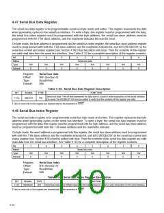
4.46 Power-Management Data Register
The power-management data register returns 0s when read, because the CardBus functions do not report dynamic
data.
Bit
7
6
5
4
3
2
1
0
Name
Type
Default
Power-management data
R
0
R
0
R
0
R
0
R
0
R
0
R
0
R
0
Register:
Offset:
Type:
Power-management data
A7h (functions 0, 1)
Read-only
Default:
00h
4−33

 TI [ TEXAS INSTRUMENTS ]