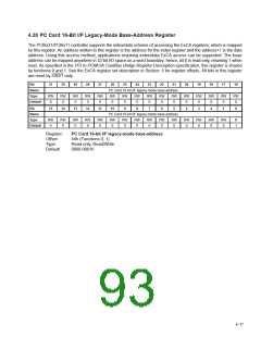
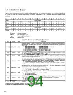
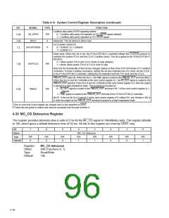
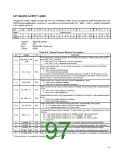
4.31 General Control Register
The general control register provides top level PCI arbitration control. It also provides the ability to disable the 1394
OHCI function and provides control over miscellaneous new functionality. See Table 4−9 for a complete description
of the register contents.
Bit
15
14
13
12
11
10
9
8
7
6
5
4
3
2
1
0
Name
Type
Default
General control
R
0
R
0
RW
0
RW
0
RW
0
RW
0
R
0
R
0
R
1
R
0
RW
0
RW
0
RW
0
R
0
RW
0
RW
0
Register:
Offset:
Type:
General control
86h
Read/Write, Read-only
0080h
Default:
Table 4−9. General Control Register Description
BIT
SIGNAL
TYPE
FUNCTION
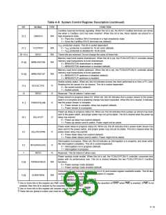
Flash media power control pin polarity. This bit controls the polarity of the MC_PWR_CTRL_0 and
MC_PWR_CTRL_1 terminals.
FM_PWR_CTRL
_POL
15 ‡
RW
0 = MC_PWR_CTRL_x terminals are active low (default)
1 = MC_PWR_CTRL_x terminals are active high
Smart Card interface select. This bit controls the selection of the dedicated Smart Card interface
used by the controller.
0 = EMV interface selected (default)
1 = PCI7x10-style interface selected
14 ‡
SC_IF_SEL
RWU
Note: The PCI7x10-style interface is only allowed when bits 9−8 (FM_IF_SEL field) are 01. If bits
9−8 contain any other value, then this bit is 0. Care must be taken in the design to ensure that this
bit can be set to 1 at the same time that bits 9−8 are set to 01.
When this bit is set, it reduces the query time for UltraMedia card types.
0 = Query time is unaffected (default)
13 ‡
12 ‡
SIM_MODE
RW
RW
1 = Query time is reduced for simulation purposes
When this bit is set, bit 0 in the I/O limit registers (PCI offsets 30h and 38h) for both CardBus functions
is set.
IO_LIMIT_SEL
0 = Bit 0 in the I/O limit registers is 0 (default)
1 = Bit 0 in the I/O limit registers is 1
When this bit is set, bit 0 in the I/O base registers (PCI offsets 2Ch and 34h) for both CardBus functions
is set.
11 ‡
10 ‡
IO_BASE_SEL
12V_SW_SEL
RW
RW
0 = Bit 0 in the I/O base registers is 0 (default)
1 = Bit 0 in the I/O base registers is 1
Power switch select. This bit selects which power switch is implemented in the system.
0 = A 1.8-V capable power switch (TPS2228) is used (default)
1 = A 12-V capable power switch (TPS2226) is used
Dedicated flash media interface selection. This field controls the mode of the dedicated flash media
interface.
00 = Flash media interface configured as SD/MMC socket + MS socket (default)
01 = Flash media interface configured as 2-in-1 (SD/MMC, MS) socket
10 = Flash media interface configured as 3-in-1 (SD/MMC, MS, SM/XD) socket
11 = Reserved
9−8 ‡
FM_IF_SEL
RW
7 ‡
6 ‡
5 ‡
4 ‡
3 ‡
DISABLE_SC
DISABLE_SD
DISABLE_FM
DISABLE_SKTB
DISABLE_OHCI
RW
RW
RW
RW
RW
When this bit is set, the Smart Card function is completely nonaccessible and nonfunctional.
When this bit is set, the SD host controller function is completely nonaccessible and nonfunctional.
When this bit is set, the flash media function is completely nonaccessible and nonfunctional.
When this bit is set, CardBus socket B (function 1) is completely nonaccessible and nonfunctional.
When this bit is set, the OHCI 1394 controller function is completely nonaccessible and nonfunctional.
‡
One or more bits in this register are cleared only by the assertion of GRST.
4−21

 TI [ TEXAS INSTRUMENTS ]