www.ti.com
ꢂ ꢀꢉ ꢠꢡꢢ ꢣ
SBOS249D − JUNE 2003− REVISED APRIL 2004
response peaking when a capacitive load is placed directly
on the output pin. When the amplifier open-loop output
resistance is considered, this capacitive load introduces
an additional pole in the signal path that can decrease the
phase margin. Several external solutions to this problem
have been suggested.
OUTPUT CURRENT AND VOLTAGE
The OPA2613 provides output voltage and current
capabilities that are unsurpassed in a low-cost dual
monolithic op amp. Under no-load conditions at 25°C, the
output voltage typically swings closer than 1V to either
supply rail; tested at +25°C, swing limit is within 1.1V of
either rail. Into a 12Ω load (the minimum tested load), it
delivers more than 280mA continuous output current.
The specifications described previously, though familiar in
the industry, consider voltage and current limits separately.
In many applications, it is the voltage times current (or V-I
product) that is more relevant to circuit operation. Refer to
the Output Voltage and Current Limitations plot in the
Typical Characteristics. The X and Y axes of this graph
show the zero-voltage output current limit and the
zero-current output voltage limit, respectively. The four
quadrants give a more detailed view of the OPA2613
output drive capabilities, noting that the graph is bounded
by a safe operating area of 1W maximum internal power
dissipation (in this case, for one channel only).
Superimposing resistor load lines onto the plot shows that
the OPA2613 can drive +4.8 and −4.1 into 25Ω without
exceeding the output capabilities or the 1W dissipation
limit. A 100Ω load line (the standard test circuit load)
shows the full 4.9V output swing capability, as shown in
the Electrical Characteristics tables. The minimum
specified output voltage and current over temperature are
set by worst-case simulations at the cold temperature
extreme. Only at cold startup will the output current and
voltage decrease to the numbers shown in the Electrical
Characteristics tables. As the output transistors deliver
power, the junction temperatures increase, decreasing the
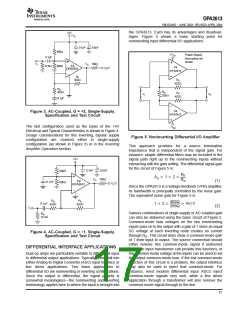
When the primary considerations are frequency response
flatness, pulse response fidelity, and/or distortion, the
simplest and most effective solution is to isolate the
capacitive load from the feedback loop by inserting a
series isolation resistor between the amplifier output and
the capacitive load. This does not eliminate the pole from
the loop response, but rather shifts it and adds a zero at a
higher frequency. The additional zero acts to cancel the
phase lag from the capacitive load pole, thus increasing
the phase margin and improving stability. The Typical
Characteristics show the Recommended RS vs Capacitive
Load and the resulting frequency response at the load.
Parasitic capacitive loads greater than 2pF can begin to
degrade the performance of the OPA2613. Long PC board
traces, unmatched cables, and connections to multiple
devices can easily cause this value to be exceeded.
Always consider this effect carefully, and add the
recommended series resistor as close as possible to the
OPA2613 output pin (see the Board Layout Guidelines
section).
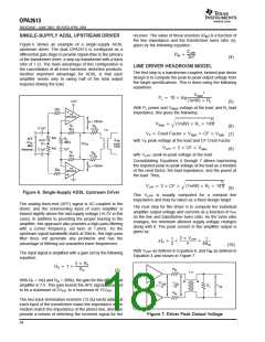
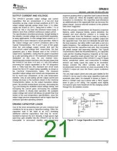
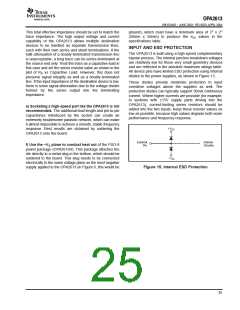
The very high output current and unity gain stability for the
OPA2613 can be used to drive large capacitive loads with
moderate slew rates. An example is shown in Figure 11
where a 5000pF load cap is driven with a 1MHz square
wave to give a 5V swing. The supplies were slightly
increased to give more headroom for the charging current
through the 2Ω isolation resistor.
V
BEs (increasing the available output voltage swing), and
increasing the current gains (increasing the available
output current). In steady-state operation, the available
output voltage and current will always be greater than that
shown in the over-temperature specifications, since the
output stage junction temperatures will be higher than the
minimum specified operating ambient.
+6.2V
Supply decoupling
not shown.
VI
2.5V
Ω
2
1/2
OPA2613
1MHz
Square
Wave
Input
VO
5000pF
DRIVING CAPACITIVE LOADS
Ω
402
One of the most demanding and yet very common load
conditions for an op amp is capacitive loading. Often, the
capacitive load is the input of an ADCincluding
additional external capacitance that may be recom-
mended to improve the ADC linearity. A high-speed, high
open-loop gain amplifier like the OPA2613 can be very
susceptible to decreased stability and closed-loop
−
6.2V
Ω
402
Figure 11. Large Capacitive Load Driver
21

 TI [ TEXAS INSTRUMENTS ]