ꢂ
ꢀꢉ
ꢠ
ꢡꢢ
ꢣ
www.ti.com
SBOS249D − JUNE 2003− REVISED APRIL 2004
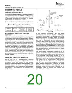
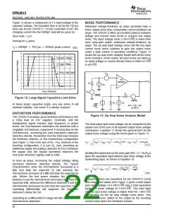
Figure 12 shows a comparison of 2 • Input voltage to the
capacitor voltage. The transition time is set by the 70V/µs
slew rate for the OPA2613. For this controlled dV/dT, the
charging current into the 5000pF load will be given by:
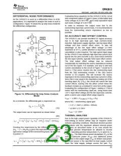
NOISE PERFORMANCE
Wideband voltage-feedback op amps generally have a
lower output noise than comparable current-feedback op
amps. The OPA2613 offers an excellent balance between
voltage and current noise terms to achieve low output
noise. The input voltage noise (1.8nV/√Hz) is lower than
most unity-gain stable, wideband voltage-feedback op
amps. The op amp input voltage noise and the two input
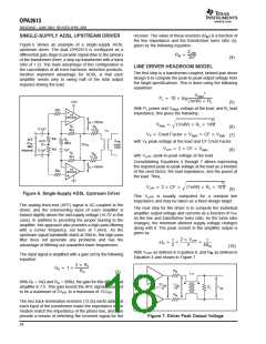
current noise terms combine to give low output noise
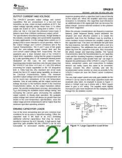
under a wide variety of operating conditions. Figure 13
shows the op amp noise analysis model with all the noise
terms included. In this model, all noise terms are taken to
be noise voltage or current density terms in either nV/√Hz
or pA/√Hz.
Slew Rate = IP/C
Solving for IP gives:
IP+ 5000pF 70Vńms + 350mA peak current
(16)
6
5
Capacitor Voltage
2X Input Voltage
4
3
2
1
0
µ
70V/ s Slew Rate
ENI
−
−
−
−
−
−
1
2
3
4
5
6
1/2
OPA2613
EO
RS
IBN
Time (100ns/div)
ERS
RF
√4kTRS
Figure 12. Large-Signal Capacitive Load Drive
√4kTRF
IBI
RG
At these larger capacitive loads, very low series R will
maintain stabilitybut some R is always required.
4kT
RG
4kT = 1.6E −20J
at 290_K
DISTORTION PERFORMANCE
Figure 13. Op Amp Noise Analysis Model
The OPA2613 provides good distortion performance into
a 100Ω load on 6V supplies. Generally, until the
fundamental signal reaches high frequency or power
levels, the 2nd-harmonic dominates the distortion with a
negligible 3rd-harmonic component. Focusing then on the
2nd-harmonic, increasing the load impedance improves
distortion directly. Remember that the total load includes
the feedback networkin the noninverting configuration
(see Figure 1), this is the sum of RF + RG, whereas in the
inverting configuration, it is just RF. Also, providing an
additional supply decoupling capacitor (0.01µF) between
the supply pins (for bipolar operation) improves the
2nd-order distortion slightly (3dB to 6dB).
The total output spot noise voltage can be computed as the
square root of the sum of all squared output noise voltage
contributors. Equation 17 shows the general form for the
output noise voltage using the terms given in Figure 13.
2
2
) ǒI
SǓ2
) ǒI
FǓ2
R ) 4kTR NG
ǒE
Ǹ
) 4kTR ǓNG
E
+
R
NI
BN
BI
F
O
S
(17)
Dividing this expression by the noise gain (NG = (1 + RF/RG))
gives the equivalent input-referred spot noise voltage at the
noninverting input, as shown in Equation 18.
In most op amps, increasing the output voltage swing
increases harmonic distortion directly. The Typical
Characteristics show the 2nd-harmonic increasing at a
little less than the expected 2x rate whereas the
3rd-harmonic increases at a little less than the expected 3x
rate. Where the test power doubles, the difference
between it and the 2nd-harmonic decreases less than the
expected 6dB, whereas the difference between it and the
3rd-harmonic decreases by less than the expected 12dB.
Operating differentially will suppress the 2nd-order
harmonics below the 3rd.
2
I
R
4kTR
NG
) ǒIBN SǓ2
NI
BI
F
F
2
+ Ǹ
) ǒ Ǔ
E
E
R
) 4kTR
)
N
S
NG
(18)
Evaluating these two equations for the OPA2613 circuit
and component values (see Figure 1) gives a total output
spot noise voltage of 6.34nV/√Hz and a total equivalent
input spot noise voltage of 3.2nV/√Hz. This total input
referred spot noise voltage is higher than the 1.8nV/√Hz
specification for the op amp voltage noise alone. This
reflects the noise added to the output by the inverting
current noise times the feedback resistor.
Operating as a differential I/O stage will also suppress the
2nd-harmonic distortion.
22

 TI [ TEXAS INSTRUMENTS ]