www.ti.com
ꢂ ꢀꢉ ꢠꢡꢢ ꢣ
SBOS249D − JUNE 2003− REVISED APRIL 2004
This total effective impedance should be set to match the
trace impedance. The high output voltage and current
capability of the OPA2613 allows multiple destination
devices to be handled as separate transmission lines,
each with their own series and shunt terminations. If the
6dB attenuation of a doubly-terminated transmission line
is unacceptable, a long trace can be series-terminated at
the source end only. Treat the trace as a capacitive load in
this case and set the series resistor value as shown in the
plot of RS vs Capacitive Load. However, this does not
preserve signal integrity as well as a doubly-terminated
line. If the input impedance of the destination device is low,
there is some signal attenuation due to the voltage divider
formed by the series output into the terminating
impedance.
ground), which must have a minimum area of 2″ x 2″
(50mm x 50mm) to produce the qJA values in the
specifications table.
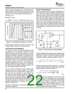
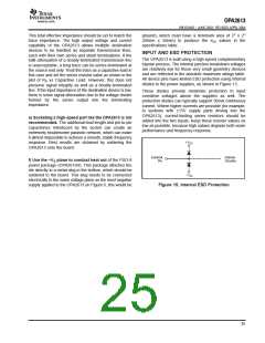
INPUT AND ESD PROTECTION
The OPA2613 is built using a high-speed complementary
bipolar process. The internal junction breakdown voltages
are relatively low for these very small geometry devices
and are reflected in the absolute maximum ratings table.
All device pins have limited ESD protection using internal
diodes to the power supplies, as shown in Figure 15.
These diodes provide moderate protection to input
overdrive voltages above the supplies as well. The
protection diodes can typically support 30mA continuous
current. Where higher currents are possible (for example,
in systems with 15V supply parts driving into the
OPA2613), current-limiting series resistors should be
added into the two inputs. Keep these resistor values as
low as possible, because high values degrade both noise
performance and frequency response.
e) Socketing a high-speed part like the OPA2613 is not
recommended. The additional lead length and pin-to-pin
capacitance introduced by the socket can create an
extremely troublesome parasitic network, which can make
it almost impossible to achieve a smooth, stable frequency
response. Best results are obtained by soldering the
OPA2613 onto the board.
+VCC
External
Pin
Internal
Circuitry
f) Use the −VS plane to conduct heat out of the PSO-8
power package (OPA2613H). This package attaches the
die directly to a metal slug in the bottom, which should be
soldered to the board. This slug needs to be connected
electrically to the same voltage plane as the most negative
supply applied to the OPA2613 (in Figure 6, this would be
−
VCC
Figure 15. Internal ESD Protection
25

 TI [ TEXAS INSTRUMENTS ]