www.ti.com
ꢂ ꢀꢉ ꢠꢡꢢ ꢣ
SBOS249D − JUNE 2003− REVISED APRIL 2004
Evaluating these equations for the OPA2613 ADSL circuit
and component values of Figure 6 gives a total output spot
noise voltage of 23.3nV/√Hz and a total equivalent input
spot noise voltage of 3.2nV/√Hz.
In order to minimize the output noise due to the
noninverting input bias current noise, it is recommended to
keep the noninverting source impedance as low as
possible.
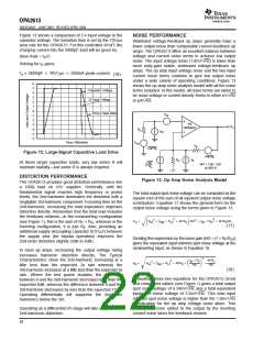
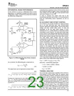
DIFFERENTIAL NOISE PERFORMANCE
As the OPA2613 is used as a differential driver in xDSL
applications, it is important to analyze the noise in such a
configuration. Figure 14 shows the op amp noise model for
the differential configuration.
IN
DC ACCURACY AND OFFSET CONTROL
Driver
The OPA2613 can provide excellent DC signal accuracy
due to its high open-loop gain, high common-mode
rejection, high power-supply rejection, and low input offset
voltage and bias current offset errors. To take full
advantage of the low input offset voltage ( 1.0mV
maximum at 25°C), careful attention to input bias current
cancellation is also required. The high-speed input stage
for the OPA2613 has relatively high input bias current (6µA
typical into the pins) but with a very close match between
the two input currents, typically 50nA input offset current.
The total output offset voltage may be reduced
considerably by matching the source impedances looking
out of the two inputs. For example, one way to add bias
current cancellation to the circuit of Figure 1 would be to
insert a 175Ω series resistor into the noninverting input
from the 50Ω terminating resistor. If the 50Ω source
resistor is DC-coupled, this will increase the source
impedance for the noninverting input bias current to 200Ω.
Since this is now equal to the impedance looking out of the
inverting input (RF || RG), the circuit will cancel the bias
current effects, leaving only the offset current times the
feedback resistor as a residual DC error term at the output.
Evaluating the configuration of Figure 1 adding a 175Ω in
series with the noninverting input pin, using worst-case
+25°C input offset voltage and the two input bias currents,
gives a worst-case output offset range equal to:
EN
RS
√4kTRF
IN
ERS
RF
√4kTRS
RG
2
EO
√4kTRG
√4kTRF
RF
IN
EN
IN
RS
ERS
√4kTRS
Figure 14. Differential Op Amp Noise Analysis
Model
VOFF
where NG = noninverting signal gain
(2 × 1.0mV) (402Ω × 300nA)
= 2.0mV 0.12mV
OFF = 2.12mV
=
(NG × VOS(MAX)
)
(IOS × RF)
As a reminder, the differential gain is expressed as:
=
2 RF
RG
GD + 1 )
(19)
(20)
V
The output noise can be expressed as shown below:
THERMAL ANALYSIS
Due to the high output power capability of the OPA2613,
heat-sinking or forced airflow may be required under
extreme operating conditions. Maximum desired junction
temperature sets the maximum allowed internal power
dissipation as described below. In no case should the
maximum junction temperature be allowed to exceed
150°C. Operating junction temperature (TJ) is given by TA
+ PD × qJA. The total internal power dissipation (PD) is the
sum of quiescent power (PDQ) and additional power
dissipation in the output stage (PDL) to deliver load power.
Quiescent power is the specified no-load supply current
times the total supply voltage across the part. PDL
) ǒiN SǓ2
) 2ǒi RFǓ2 ) 2ǒ4kTR DǓ
2
2
e
+
2 G
ǒ
e
R
) 4kTR
Ǔ
G
Ǹ
D
N
I
F
O
S
Dividing this expression by the differential noise gain
(GD = (1 + 2RF/RG)) gives the equivalent input referred
spot noise voltage at the noninverting input, as shown in
Equation 21.
(21)
2
SǓ2
R
i R
4kTR
F
I
F
2
) ǒi
N
e + Ǹ
ǒe
) 4kTR Ǔ) 2ǒ Ǔ ) 2ǒ Ǔ
2
i
N
S
G
G
D
D
23

 TI [ TEXAS INSTRUMENTS ]