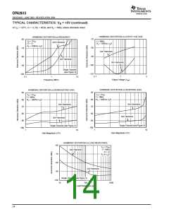
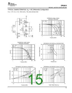
ꢂ
ꢀ
ꢉ
ꢠ
ꢡ
ꢢ
ꢣ
www.ti.com
SBOS249D − JUNE 2003− REVISED APRIL 2004
receiver. The value of these resistors (RM) is a function of
the line impedance and the transformer turns ratio (n),
given by the following equation:
SINGLE-SUPPLY ADSL UPSTREAM DRIVER
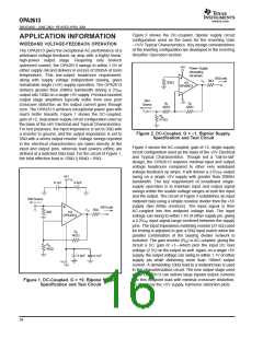
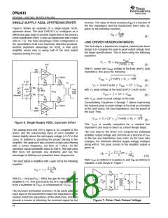
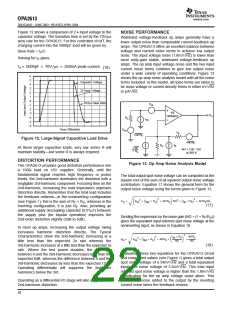
Figure 6 shows an example of a single-supply ADSL
upstream driver. The dual OPA2613 is configured as a
differential gain stage to provide signal drive to the primary
of the transformer (here, a step-up transformer with a turns
ratio of 1:2). The main advantage of this configuration is
the cancellation of all even harmonic distortion products.
Another important advantage for ADSL is that each
amplifier needs only to swing half of the total output
required driving the load.
ZLINE
2n2
RM +
(4)
LINE DRIVER HEADROOM MODEL
The first step in a transformer-coupled, twisted-pair driver
design is to compute the peak-to-peak output voltage from
the target specifications. This is done using the following
equations:
2
VRMS
PL + 10 log
(1mW) RL
+12V
(5)
With PL power and VRMS voltage at the load, and RL load
impedance, this gives the following:
20
Ω
1/2
OPA2613
P
L
IP = 150mA
RM
+ Ǹ
VRMS
(1mW) RL 1010
RF
1k
Ω
(6)
(7)
0.1 F
µ
12.5
Ω
1:n
VP + Crest Factor VRMS + CF VRMS
1k
Ω
RG
308
AFE
2VPP
Max
ZLINE
100
+6.3V
with VP peak voltage at the load and CF Crest Factor.
LPP + 2 CF VRMS
with VLPP: peak-to-peak voltage at the load.
Ω
15VPP
Ω
V
1k
Ω
1 F
µ
(8)
0.1 F
µ
Assumed
RF
1k
RM
12.5
Ω
Ω
Consolidating Equations 4 through 7 allows expressing
the required peak-to-peak voltage at the load as a function
of the crest factor, the load impedance, and the power at
the load. Thus,
IP = 150mA
1/2
OPA2613
20
Ω
P
L
Ǹ
V
LPP + 2 CF (1mW) RL 1010
(9)
Figure 6. Single-Supply ADSL Upstream Driver
This VLPP is usually computed for a nominal line
impedance and may be taken as a fixed design target.
The analog front-end (AFE) signal is AC-coupled to the
driver, and the noninverting input of each amplifier is
biased slightly above the mid-supply voltage (+6.3V in this
case). In addition to providing the proper biasing to the
amplifier, this approach also provides a high-pass filtering
with a corner frequency, set here at 1.6kHz. As the
upstream signal bandwidth starts at 26kHz, this high-pass
filter does not generate any problems and has the
advantage of filtering out unwanted lower frequencies.
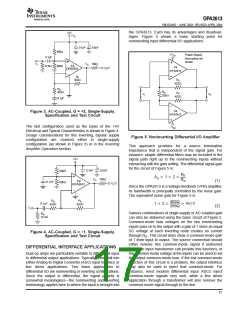
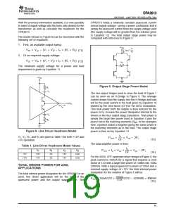
The next step for the driver is to compute the individual
amplifier output voltage and currents as a function of VPP
on the line and transformer turns ratio. As the turns ratio
changes, the minimum allowed supply voltage changes
along with it. The peak current in the amplifier output is
given by:
2 VLPP
1
2
1
4RM
"IP +
n
(10)
With VLPP as defined in Equation 8, and RM as defined in
Equation 4 and shown in Figure 7.
The input signal is amplified with a gain set by the following
equation:
2 RF
RG
GD + 1 )
RM
(3)
1:n
With RF = 1kΩ and RG = 308Ω, the gain for this differential
amplifier is 7.5. This gain boosts the AFE signal, assumed
2VLpp
=
n
VLpp
n
RL
VLpp
Vpp
to be a maximum of 2VPP, to a maximum of 15VPP
.
RM
The two back-termination resistors (12.5Ω each) added at
each input of the transformer make the impedance of the
modem match the impedance of the phone line, and also
provide a means of detecting the received signal for the
Figure 7. Driver Peak Output Voltage
18

 TI [ TEXAS INSTRUMENTS ]