www.ti.com
ꢂ ꢀꢉ ꢠꢡꢢ ꢣ
SBOS249D − JUNE 2003− REVISED APRIL 2004
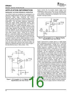
the OPA2613. Each has its advantages and disadvan-
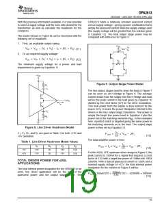
tages. Figure 5 shows a basic starting point for
noninverting input differential I/O applications.
+5V
+VS
+
0.1 F
µ
6.8 F
µ
806
Ω
+VCC
Power−Supply
decoupling not
shown.
0.1 F
µ
VI
VO 100
Ω
1/2
OPA2613
57.6
806
Ω
Ω
1/2
VS /2
OPA2613
RF
402
RF
Ω
Ω
402
RG
402
RG
268
Ω
RF
VI
VO
Ω
Ω
402
0.1 F
µ
1/2
OPA2613
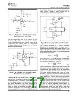
Figure 3. AC-Coupled, G = +2, Single-Supply,
Specification and Test Circuit
The last configuration used as the basis of the +5V
Electrical and Typical Characteristics is shown in Figure 4.
Design considerations for this inverting, bipolar supply
configuration are covered either in single-supply
configuration (as shown in Figure 3) or in the Inverting
Amplifier Operation section.
−
VCC
Figure 5. Noninverting Differential I/O Amplifier
This approach provides for source termination
impedance that is independent of the signal gain. For
instance, simple differential filters may be included in the
signal path right up to the noninverting inputs without
interacting with the gain setting. The differential signal gain
for the circuit of Figure 5 is:
a
+5V
+
µ
µ
6.8 F
0.1 F
Ω
Ω
806
806
RF
RG
AD + 1 ) 2
Ω
VO 100
(1)
1/2
OPA2613
µ
0.1 F
VS /2
Since the OPA2613 is a voltage-feedback (VFB) amplifier,
its bandwidth is principally controlled by the noise gain.
The equivalent noise gain for Figure 5 is:
RG
RF
Ω
402
402W
268W
µ
0.1 F
1 ) 2
+ 4VńV
Ω
402
(2)
VI
Various combinations of single-supply or AC-coupled gain
can also be delivered using the basic circuit of Figure 5.
Common-mode bias voltages on the two noninverting
inputs pass on to the output with a gain of 1 since an equal
DC voltage at each inverting node creates no current
through RG. This circuit does show a common-mode gain
of 1 from input to output. The source connection should
either remove this common-mode signal if undesired
(using an input transformer can provide this function), or
the common-mode voltage at the inputs can be used to set
the output common-mode bias. If the low common-mode
rejection of this circuit is a problem, the output interface
may also be used to reject that common-mode. For
instance, most modern differential input ADCs reject
common-mode signals very well, while a line driver
application through a transformer will also remove the
common-mode signal through to the line.
RM
57.6
Ω
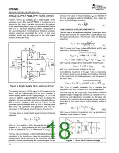
Figure 4. AC-Coupled, G = −1, Single-Supply,
Specification and Test Circuit
DIFFERENTIAL INTERFACE APPLICATIONS
Dual op amps are particularly suitable to differential input
to differential output applications. Typically, these fall into
either Analog-to-Digital Converter (ADC) input interface or
line driver applications. Two basic approaches to
differential I/O are noninverting or inverting configurations.
Since the output is differential, the signal polarity is
somewhat meaningless—the noninverting and inverting
terminology applies here to where the input is brought into
17

 TI [ TEXAS INSTRUMENTS ]