ꢂ
ꢀꢉ
ꢠ
ꢡꢢ
ꢣ
www.ti.com
SBOS249D − JUNE 2003− REVISED APRIL 2004
depends on the required output signal and load, but for a
grounded resistive load, PDL is at a maximum when the
output is fixed at a voltage equal to 1/2 of either supply
voltage (for equal bipolar supplies). Under this condition,
PDL = VS2/(4 × RL) where RL includes feedback network
loading. Note that it is the power in the output stage and not
into the load that determines internal power dissipation. As
a worst-case example, compute the maximum TJ using an
OPA2613 SO-8 in the circuit of Figure 1 operating at the
maximum specified ambient temperature of +85°C with
both outputs driving a grounded 20Ω load to +3.0V.
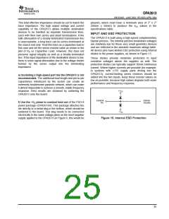
c) Careful selection and placement of external
components preserve the high-frequency performance
of the OPA2613. Resistors should be of a very low
reactance type. Surface-mount resistors work best and
allow a tighter overall layout. Metal film and carbon
composition axially leaded resistors can also provide good
high-frequency performance. Again, keep the leads and
PC board trace length as short as possible. Never use
wire-wound type resistors in a high-frequency application.
Although the output pin and inverting input pin are the most
sensitive to parasitic capacitance, always position the
feedback and series output resistor, if any, as close as
possible to the output pin. Other network components,
such as noninverting input termination resistors, should
also be placed close to the package. Where double-side
component mounting is allowed, place the feedback
resistor directly under the package on the other side of the
board between the output and inverting input pins. The
402Ω feedback resistor used in the Typical Characteristics
at a gain of +2 on 6V supplies is a good starting point for
design.
PD = 12V × 13.0mA + 2 × [62/ (4 × (20Ω 804Ω))] = 1. 08W
Maximum TJ = +85°C + (1.08W × 125°C/W) = 220°C
This absolute worst-case condition exceeds specified
maximum junction temperature. This extreme case is not
normally encountered. Where high internal power dissipa-
tion is anticipated, consider the thermal slug package
version. Under the same worst case conditions the
junction temperature will drop to 139°C with the 50°C/W
thermal impedance available using the PSO-8 package.
d) Connections to other wideband devices on the board
may be made with short direct traces or through onboard
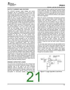
transmission lines. For short connections, consider the
trace and the input to the next device as a lumped
capacitive load. Relatively wide traces (50mils to 100mils)
should be used, preferably with ground and power planes
opened up around them. Estimate the total capacitive load
and set RS from the plot of Recommended RS vs
Capacitive Load. Low parasitic capacitive loads (< 5pF)
may not need an RS because the OPA2613 is nominally
compensated to operate with a 2pF parasitic load. If a long
trace is required, and the 6dB signal loss intrinsic to a
doubly-terminated transmission line is acceptable,
implement a matched impedance transmission line using
microstrip or stripline techniques (consult an ECL design
handbook for microstrip and stripline layout techniques). A
50Ω environment is normally not necessary on board; in
fact, a higher impedance environment improves distortion
(see the distortion versus load plots). With a characteristic
board trace impedance defined based on board material
and trace dimensions, a matching series resistor into the
trace from the output of the OPA2613 is used, as well as
a terminating shunt resistor at the input of the destination
device. Remember also that the terminating impedance is
the parallel combination of the shunt resistor and the input
impedance of the destination device.
BOARD LAYOUT GUIDELINES
Achieving optimum performance with a high-frequency
amplifier like the OPA2613 requires careful attention to
board layout parasitic and external component types.
Recommendations that optimize performance include:
a) Minimize parasitic capacitance to any AC ground for
all of the signal I/O pins. Parasitic capacitance on the
output and inverting input pins can cause instability; on the
noninverting input, it can react with the source impedance
to cause unintentional band limiting. To reduce unwanted
capacitance, a window around the signal I/O pins should
be opened in all of the ground and power planes around
those pins. Otherwise, ground and power planes should
be unbroken elsewhere on the board.
b) Minimize the distance (< 0.25″) from the power-supply
pins to high-frequency 0.1µF decoupling capacitors. At the
device pins, the ground and power plane layout should not
be in close proximity to the signal I/O pins. Avoid narrow
power and ground traces to minimize inductance between
the pins and the decoupling capacitors. The power-supply
connections (on pins 4 and 7) should always be decoupled
with these capacitors. An optional supply decoupling
capacitor across the two power supplies (for bipolar
operation) improves 2nd-harmonic distortion performance.
Larger (2.2µF to 6.8µF) decoupling capacitors, effective at
a lower frequency, should also be used on the main supply
pins. These can be placed somewhat farther from the
device and may be shared among several devices in the
same area of the PC board.
24

 TI [ TEXAS INSTRUMENTS ]