www.ti.com
ꢂ ꢀꢉ ꢠꢡꢢ ꢣ
SBOS249D − JUNE 2003− REVISED APRIL 2004
With the previous information available, it is now possible
to select a supply voltage and the turns ratio desired for the
transformer as well as calculate the headroom for the
OPA2613.
OPA2613 holds a relatively constant quiescent current
versus supply voltage—giving a power contribution that is
simply the quiescent current times the supply voltage used
(the supply voltage will be greater than the solution given
in Equation 12). The total output stage power may be
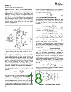
computed with reference to Figure 9.
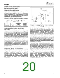
The model (shown in Figure 8) can be described with the
following set of equations:
1. First, as available output swing:
+VCC
IP
IAVG
=
V
PP + VCC * (V1 ) V2) * IP (R1 ) R2)
(11)
(12)
CF
2. Or as required supply voltage:
VCC + VPP ) (V1 ) V2) ) IP (R1 ) R2)
RT
The minimum supply voltage for a power and load
requirement is given by Equation 11.
+VCC
Figure 9. Output Stage Power Model
R1
V1
The two output stages used to drive the load of Figure 7
can be seen as an H-Bridge in Figure 9. The average
current drawn from the supply into this H-Bridge and load
will be the peak current in the load given by Equation 10
divided by the crest factor (CF) for the xDSL modulation.
This total power from the supply is then reduced by the
power in RT to leave the power dissipated internal to the
drivers in the four output stage transistors. That power is
simply the target line power used in Equation 5 plus the
power lost in the matching elements (RM). In the examples
here, a perfect match is targeted giving the same power in
the matching elements as in the load. The output stage
power is then set by Equation 13.
VO
IP
V2
R2
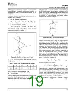
Figure 8. Line Driver Headroom Model
IP
CF
V1, V2, R1, and R2 are given in Table 1 for both +12V and
+5V operation.
POUT
+
VCC * 2PL
(13)
The total amplifier power is then:
IP
Table 1. Line Driver Headroom Model Values
V
R
V
R
2
PTOT + Iq VCC
)
VCC * 2PL
1
1
2
CF
(14)
+5V
1.0V
1.0V
2Ω
2Ω
1.0V
1.0V
5.5Ω
5.5Ω
For the ADSL CPE upstream driver design of Figure 6, the
peak current is 150mA for a signal that requires a crest
factor of 5.33 with a target line power of 13dBm into 100Ω
(20mW). With a typical quiescent current of 12mA and a
nominal supply voltage of +12V, the total internal power
dissipation for the solution of Figure 6 will be:
+12V
TOTAL DRIVER POWER FOR xDSL
APPLICATIONS
The total internal power dissipation for the OPA2613 in an
xDSL line driver application will be the sum of the
quiescent power and the output stage power. The
150mA
5.33
(
)
(
)
(
)
P
TOT + 12mA 12V )
12V * 2 20mW + 400mW
(15)
19

 TI [ TEXAS INSTRUMENTS ]