ONET1131EC
www.ti.com.cn
ZHCSFG0 –SEPTEMBER 2016
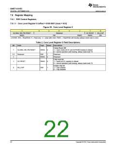
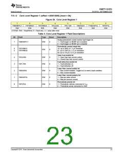
7.6.1.2 Core Level Register 1 (offset = 0000 0000) [reset = 0h]
Figure 26. Core Level Register 1
7
6
5
4
3
2
1
0
TXMONPFLT
R/W
TXPDRNG1
R/W
TXPDRNG0
R/W
TXOLENA
R/W
TXFLTEN
R/W
TXBIASEN
R/W
TTXBIASPOL
R/W
TXPDPOL
R/W
LEGEND: R/W = Read/Write; R = Read only; -n = value after reset
Table 3. Core Level Register 1 Field Descriptions
Bit
Field
Type
Reset
Description
Analog photodiode current monitor fault trigger bit
1 = Fault trigger on MONP pin is enabled
0 = Fault trigger on MONP pin is disabled
7
TXMONPFLT
R/W
0
Photodiode current range bits
1X: up to 3080 μA / 3 μA resolution
01: up to 1540 μA / 1.5 μA resolution
00: up to 770 μA / 0.75 μA resolution
6
5
TXPDRNG1
TXPDRNG0
R/W
0
Open loop enable bit
4
3
2
1
0
TXOLENA
TXFLTEN
TXBIASEN
TXBIASPOL
TXPDPOL
R/W
R/W
R/W
R/W
R/W
0
0
0
0
0
1 = Open loop bias current control
0 = Closed loop bias current control
Fault detection enable bit
1 = Fault detection on
0 = Fault detection off
Laser Bias current enable bit
1 = Bias current enabled. Toggle to 0 to reset a fault condition.
0 = Bias current disabled
Laser Bias current polarity bit
1 = Bias pin sinks current
0 = Bias pin sources current
Photodiode polarity bit
1 = Photodiode cathode connected to VCC
0 = Photodiode anode connected to GND
Copyright © 2016, Texas Instruments Incorporated
23

 TI [ TEXAS INSTRUMENTS ]