ONET1131EC
ZHCSFG0 –SEPTEMBER 2016
www.ti.com.cn
7.6.3 TX Registers
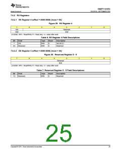
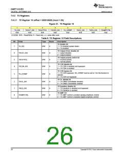
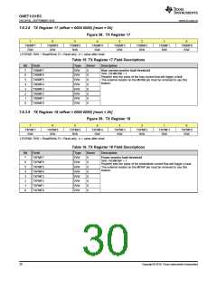
7.6.3.1 TX Register 10 (offset = 0000 0000) [reset = 0h]
Figure 31. TX Register 10
7
6
5
4
3
2
1
0
TX_DIS
R/W
TXOUT_DIS
R/W
TXOUTPOL
R/W
TXCDR_DIS
R/W
TX_CDRBP
R/W
TXOC_DIS
R/W
TXEQ_DIS
R/W
TXAMPCTRL
R/W
LEGEND: R/W = Read/Write; R = Read only; -n = value after reset
Table 8. TX Register 10 Field Descriptions
Bit
Field
Type
Reset
Description
TX disable bit
7
TX_DIS
R/W
0
1 = TX disabled (power-down)
0 = TX enabled
TX Output Driver disable bit
1 = output disabled
0 = output enabled
6
5
4
TXOUT_DIS
TXOUTPOL
TXCDR_DIS
R/W
R/W
R/W
0
0
0
TX Output polarity switch bit
1 = inverted polarity
0 = normal polarity
TX CDR disable bit
1 = TX CDR is disabled and bypassed
0 = TX CDR is enabled
TX CDR bypass bit
1 = TX-CDR bypassed. RX_CDRBP must be set to 1 for this function to
operate.
3
TX_CDRBP
R/W
0
0 = TX-CDR not bypassed
TX OC disable bit
2
1
0
TXOC_DIS
TXEQ_DIS
TXAMPCTRL
R/W
R/W
R/W
0
0
0
1 = TX Offset Cancellation disabled
0 = TX Offset Cancellation enabled
TX Equalizer disable bit
1 = TX Equalizer is disabled and bypassed
0 = TX Equalizer is enabled
TX AMP Ctrl
1 = TX AMP Control is enabled (analog amplitude control)
0 = TX AMP Control is disabled (digital amplitude control)
26
Copyright © 2016, Texas Instruments Incorporated

 TI [ TEXAS INSTRUMENTS ]