ONET1131EC
www.ti.com.cn
ZHCSFG0 –SEPTEMBER 2016
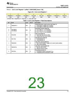
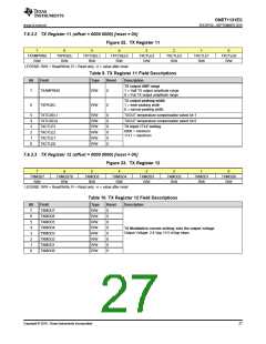
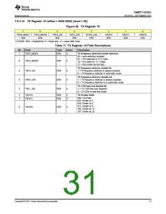
7.6.3.2 TX Register 11 (offset = 0000 0000) [reset = 0h]
Figure 32. TX Register 11
7
6
5
4
3
2
1
0
TXAMPRNG
R/W
TXPKSEL
R/W
TXTCSEL1
R/W
TXTCSEL0
R/W
TXCTLE3
R/W
TXCTLE2
R/W
TXCTLE1
R/W
TXCTLE0
R/W
LEGEND: R/W = Read/Write; R = Read only; -n = value after reset
Table 9. TX Register 11 Field Descriptions
Bit
Field
Type
Reset
Description
TX output AMP range
7
TXAMPRNG
R/W
0
1 = Half TX output amplitude range
0 = Full TX output amplitude range
TX output peaking width
1 = wide peaking width
0 = narrow peaking width
6
TXPKSEL
R/W
0
5
4
3
2
1
0
TXTCSEL1
TXTCSEL0
TXCTLE3
TXCTLE2
TXCTLE1
TXCTLE0
R/W
R/W
R/W
R/W
R/W
R/W
0
0
0
0
0
0
TXOUT temperature compensation select bit 1
TXOUT temperature compensation select bit 0
TX input CTLE setting
0000 = minimum
1111 = maximum
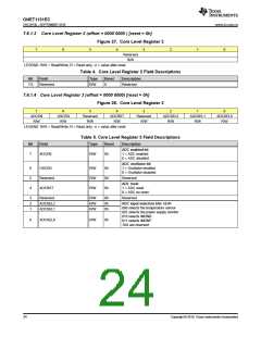
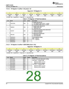
7.6.3.3 TX Register 12 (offset = 0000 0000) [reset = 0h]
Figure 33. TX Register 12
7
6
5
4
3
2
1
0
TXMOD7
R/W
TXMOD76
R/W
TXMOD5
R/W
TXMOD4
R/W
TXMOD3
R/W
TXMOD2
R/W
TXMOD1
R/W
TXMOD0
R/W
LEGEND: R/W = Read/Write; R = Read only; -n = value after reset
Table 10. TX Register 12 Field Descriptions
Bit
7
Field
Type
R/W
R/W
R/W
R/W
R/W
R/W
R/W
R/W
Reset
Description
TXMOD7
TXMOD6
TXMOD5
TXMOD4
TXMOD3
TXMOD2
TXMOD1
TXMOD0
0
0
0
0
0
0
0
0
6
5
4
TX Modulation current setting: sets the output voltage
Output Voltage: 2.4 Vpp / 9.5 mVpp steps
3
2
1
0
Copyright © 2016, Texas Instruments Incorporated
27

 TI [ TEXAS INSTRUMENTS ]