ONET1131EC
ZHCSFG0 –SEPTEMBER 2016
www.ti.com.cn
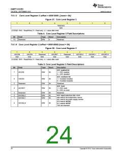
To digitally monitor the photodiode current, ensure that TXDMONP = 1 (bit 6 of register 16) and that a resistor is
not connected to the MONP pin. To digitally monitor the bias current, ensure that TXDMONB = 1 (bit 5 of register
16) and that a resistor is not connected to the MONB pin. The ADC is disabled by default. To enable the ADC,
set the ADC oscillator enable bit OSCEN = 1 (bit 6 of register 3) and set the ADC enable bit ADCEN = 1 (bit 7 of
register 3).
The digital word read from the ADC can be converted to its analog equivalent through the following formulas.
7.3.8.3.1 Temperature
Temperature (°C) = (0.5475 × ADCx) – 273
(1)
(2)
7.3.8.3.2 Power Supply Voltage
Power supply voltage (V) = (1.36m × ADCx) + 1.76
7.3.8.3.3 Photodiode Current Monitor
IPD(μA) = 2 x [ (0.62 × ADCx) – 16] for TXPDRNG00
IPD(μA) = 4 x [ (0.62 × ADCx) – 16] for TXPDRNG01
IPD(μA) = 8 x [ (0.62 × ADCx) – 16] for TXPDRNG1x
(3)
(4)
(5)
7.3.8.3.4 Bias Current Monitor
IBIAS (mA) = (0.2 × ADCx) – 4.5
(6)
Where: ADCx = the decimal value read from the ADC
7.3.8.4 2-Wire Interface and Control Logic
The ONET1131EC uses a 2-wire serial interface for digital control. The two circuit inputs, SDA and SCK, are
driven, respectively, by the serial data and serial clock from a microprocessor, for example. The SDA and SCK
pins require external 4.7-kΩ to 10-kΩ pull-up resistor to VCC for proper operation.
The 2-wire interface allows write access to the internal memory map to modify control registers and read access
to read out the control signals. The ONET1131EC is a slave device only which means that it cannot initiate a
transmission itself; it always relies on the availability of the SCK signal for the duration of the transmission. The
master device provides the clock signal as well as the START and STOP commands. The protocol for a data
transmission is as follows:
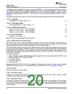
1. START command
2. Seven (7) bit slave address (0001000) followed by an eighth bit which is the data direction bit (R/W). A zero
indicates a WRITE and a 1 indicates a READ.
3. 8 bit register address
4. 8 bit register data word
5. STOP command
Regarding timing, the ONET1131EC is I2C compatible. The typical timing is shown in Figure 2 and a complete
data transfer is shown in Figure 24. Parameters for Figure 2 are defined in the Timing Diagram Definitions.
7.3.8.5 Bus Idle
Both SDA and SCK lines remain HIGH
7.3.8.6 Start Data Transfer
A change in the state of the SDA line, from HIGH to LOW, while the SCK line is HIGH, defines a START
condition (S). Each data transfer is initiated with a START condition.
7.3.8.7 Stop Data Transfer
A change in the state of the SDA line from LOW to HIGH while the SCK line is HIGH defines a STOP condition
(P). Each data transfer is terminated with a STOP condition; however, if the master still wishes to communicate
on the bus, it can generate a repeated START condition and address another slave without first generating a
STOP condition.
20
Copyright © 2016, Texas Instruments Incorporated

 TI [ TEXAS INSTRUMENTS ]