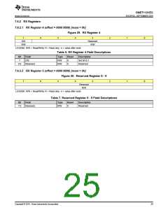
ONET1131EC
www.ti.com.cn
ZHCSFG0 –SEPTEMBER 2016
7.3.8.8 Data Transfer
Only one data byte can be transferred between a START and a STOP condition. The receiver acknowledges the
transfer of data.
7.3.9 Acknowledge
Each receiving device, when addressed, is obliged to generate an acknowledge bit. The transmitter releases the
SDA line and a device that acknowledges must pull down the SDA line during the acknowledge clock pulse in
such a way that the SDA line is stable LOW during the HIGH period of the acknowledge clock pulse. Setup and
hold times must be taken into account. When a slave-receiver doesn’t acknowledge the slave address, the data
line must be left HIGH by the slave. The master can then generate a STOP condition to abort the transfer. If the
slave-receiver does acknowledge the slave address but some time later in the transfer cannot receive any more
data bytes, the master must abort the transfer. This is indicated by the slave generating the not acknowledge on
the first byte to follow. The slave leaves the data line HIGH and the master generates the STOP condition, see
Figure 2.
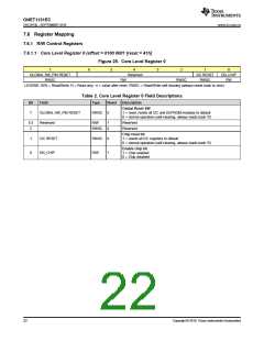
7.4 Device Functional Modes
The ONET1131EC has two main functional modes of operation: differential transmitter output and single-ended
transmitter output.
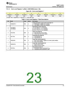
7.4.1 Differential Transmitter Output
Operation with differential output is the default mode of operation. This mode is intended for externally modulated
lasers requiring differential drive such as Mach Zehnder modulators.
7.4.2 Single-Ended Transmitter Output
In order to reduce the power consumption for single-ended EML applications the output driver should be set to
single-ended mode. The single-ended output signal can be enabled by setting the transmitter mode select bit
TXMODE = 1 (bit 6 of register 13). The positive output is active by default. To enable the negative output and
disable the positive output set TXOUTSEL = 1 (bit 7 of register 13).
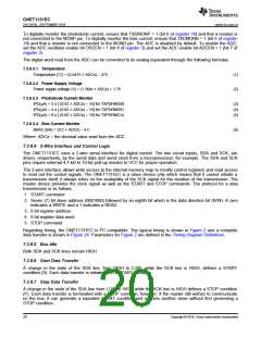
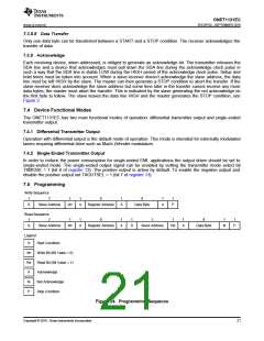
7.5 Programming
Write Sequence
1
1
1
8
1
8
1
1
7
S
Slave Address
Wr
A
Register Address
A
Data Byte
A
P
Read Sequence
1
1
1
8
1
1
1
1
8
1
1
7
7
S
Slave Address
Wr
A
Register Address
A
S
Slave Address
Rd
A
Data Byte
N
P
Legend
S
Start Condition
Wr
Rd
A
Write Bit (Bit Value = 0)
Read Bit (Bit Value = 1)
Acknowledge
N
Not Acknowledge
Stop Condition
P
Figure 24. Programming Sequence
Copyright © 2016, Texas Instruments Incorporated
21

 TI [ TEXAS INSTRUMENTS ]