ONET1131EC
ZHCSFG0 –SEPTEMBER 2016
www.ti.com.cn
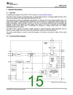
7.3 Feature Description
7.3.1 Equalizer
The data signal is applied to an input equalizer by means of the input signal pins DIN+ / DIN–, which provide on-
chip differential 100-Ω line termination. The equalizer is enabled by default and can be disabled by setting the
transmitter equalizer disable bit TXEQ_DIS = 1 (bit 1 of register 10). Equalization of up to 300 mm (12 inches) of
microstrip or stripline transmission line on FR4 printed circuit boards can be achieved. The amount of
equalization is set through register settings TXCTLE [0..3] (register 11). The device can accept input amplitude
levels from 100 mVpp up to 1000 mVpp.
7.3.2 CDR
The clock and data recovery function consists of a Phase-Locked Loop (PLL) and retimer. The CDR can be
operated without a reference clock and the Voltage Controlled Oscillator (VCO) can cover 9.8 Gbps to 11.7 Gbps
data rates. The PLL is phase locked to the incoming data stream and attenuates the high frequency jitter on the
data, producing a recovered clean clock with substantially reduced jitter. An external capacitor for the PLL loop
filter is connected to the LF pin. A value of 2.2 nF is recommended. The clean clock is used to retime the
incoming data, producing an output signal with reduced jitter, and in effect, resetting the jitter budget for the
transmitter.
The CDR is enabled by default. The CDR can be disabled and bypassed by setting the transmitter CDR disable
bit TXCDR_DIS = 1 (bit 4 of register 10). Alternatively, the CDR can be left powered on but bypassed by setting
the transmitter CDR bypass bit TX_CDRBP = 1 (bit 3 of register 10); however, this function only works if the
receiver CDR bypass bit RX_CDRBP (bit 3 of register 4) is also set to 1.
The CDR is designed to meet the XFP Datacom requirements and Telecom requirements for a maximum of 1-dB
jitter peaking at a frequency greater than 120 kHz. The CDR is not designed to meet the Telecom regenerator
requirements of jitter peaking less than 0.03 dB at a frequency less than 120 kHz. The default CDR bandwidth is
typically 4.5 MHz and can be adjusted using the SEL_RES[0..2] bits (bits 5 to 7 of register 51). Adjusting these
bits changes the bandwidth of both the transmitter and receiver CDRs.
For the majority of applications, the default settings in register 19 for the transmitter CDR can be used. However,
for some applications or for test purposes, some modes of operation may be useful. The frequency detector for
the PLL is set to an automatic mode of operation by default. When a signal is applied to the transmitter input the
frequency detector search algorithm will be initiated to determine the frequency of the data. The default algorithm
ensures a fast CDR lock time of less than 2 ms. The fast lock can be disabled by setting the transmitter CDR fast
lock disable bit TXFL_DIS = 1 (bit 3 of register 19). Once the frequency has been detected then the frequency
detector will be disabled and the supply current will decrease by approximately 10mA. In some applications, such
as when there are long periods of idle data, it may be advantageous to keep the frequency detector permanently
enabled by setting the transmitter frequency detector enable bit TXFD_EN = 1 (bit 5 of register 19). For test
purposes, the frequency detector can be permanently disabled by setting the transmitter frequency detector
disable bit TXFD_DIS = 1 (bit 4 of register 19). For fast lock times the frequency detector can be set to one of
two preselected data rates using the transmitter frequency detection mode selection bits TXFD_MOD[0..1] (bits 6
and 7 of register 19). If it is desired to use the retimer at lower data rates than the standard 9.8 to 11.7Gbps then
the transmitter divider ratio should be adjusted accordingly through TXDIV[0..2] (bits 0 to 2 of register 19). For
example, for re-timed operation at 2.5 Gbps the divider should be set to divide by 4.
7.3.3 Modulator Driver
The modulation current is sunk from the common emitter node of the limiting output driver differential pair by
means of a modulation current generator, which is digitally controlled by the 2-wire serial interface.
The collector nodes of the output stages are connected to the transmitter output pins TXOUT+ and TXOUT–.
The collectors have internal 50Ω back termination resistors to VCC_TX. The outputs are optimized to drive a 50
Ω single-ended load and to obtain the maximum single-ended output voltage of 2.0Vpp, AC coupling and
inductive pull-ups to VCC are required. For reduced power consumption the DC resistance of the inductive pull-
ups should be minimized to provide sufficient headroom on the TXOUT+ and TXOUT– pins.
The polarity of the output pins can be inverted by setting the transmitter output polarity switch bit, TXOUTPOL
(bit 5 of register 10) to 1. In addition, the output driver can be disabled by setting the transmitter output driver
disable bit TXOUT_DIS = 1 (bit 6 of register 10).
16
Copyright © 2016, Texas Instruments Incorporated

 TI [ TEXAS INSTRUMENTS ]