MSP430F530x, MSP430F5310
SLAS677B –SEPTEMBER 2010–REVISED MARCH 2011
www.ti.com
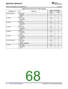
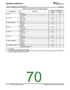
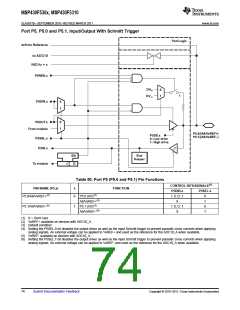
Table 47. Port P2 (P2.0 to P2.7) Pin Functions
CONTROL BITS/SIGNALS(1)
PIN NAME (P2.x)
P2.0/TA1.1
x
FUNCTION
P2DIR.x
P2SEL.x
0
P2.0 (I/O)
TA1.CCI1A
TA1.1
I: 0; O: 1
0
1
1
0
1
1
0
1
1
0
1
1
0
1
1
0
1
1
0
1
1
0
1
0
1
P2.1/TA1.2
1
2
3
4
5
6
7
P2.1 (I/O)
TA1.CCI2A
TA1.2
I: 0; O: 1
0
1
P2.2/TA2CLK/SMCLK
P2.3/TA2.0
P2.2 (I/O)
TA2CLK
I: 0; O: 1
0
SMCLK
1
P2.3 (I/O)
TA2.CCI0A
TA2.0
I: 0; O: 1
0
1
P2.4/TA2.1
P2.4 (I/O)
TA2.CCI1A
TA2.1
I: 0; O: 1
0
1
P2.5/TA2.2
P2.5 (I/O)
TA2.CCI2A
TA2.2
I: 0; O: 1
0
1
P2.6/RTCCLK/DMAE0
P2.6 (I/O)
DMAE0
I: 0; O: 1
0
RTCCLK
P2.7 (I/O)
UCB0STE/UCA0CLK(2) (3)
1
I: 0; O: 1
X
P2.7/UCB0STE/UCA0CLK
(1) X = Don't care
(2) The pin direction is controlled by the USCI module.
(3) UCA0CLK function takes precedence over UCB0STE function. If the pin is required as UCA0CLK input or output, USCI A0/B0 is forced
to 3-wire SPI mode if 4-wire SPI mode is selected.
70
Submit Documentation Feedback
Copyright © 2010–2011, Texas Instruments Incorporated

 TI [ TEXAS INSTRUMENTS ]