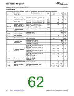
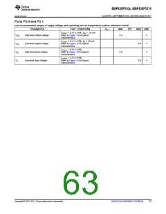
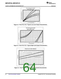
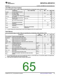
MSP430F530x, MSP430F5310
SLAS677B –SEPTEMBER 2010–REVISED MARCH 2011
www.ti.com
JTAG and Spy-Bi-Wire Interface
over recommended ranges of supply voltage and operating free-air temperature (unless otherwise noted)
TEST
CONDITIONS
PARAMETER
MIN
TYP
MAX UNIT
fSBW
Spy-Bi-Wire input frequency
2.2 V/3 V
0
20 MHz
tSBW,Low
Spy-Bi-Wire low clock pulse length
2.2 V/3 V
0.025
15
µs
Spy-Bi-Wire enable time (TEST high to acceptance of first clock
edge)
tSBW, En
tSBW,Rst
2.2 V/3 V
1
µs
(1)
Spy-Bi-Wire return to normal operation time
15
0
100
5
µs
2.2 V
3 V
MHz
(2)
fTCK
TCK input frequency - 4-wire JTAG
0
10 MHz
80 kΩ
Rinternal
Internal pulldown resistance on TEST
2.2 V/3 V
45
60
(1) Tools accessing the Spy-Bi-Wire interface need to wait for the tSBW,En time after pulling the TEST/SBWTCK pin high before applying the
first SBWTCK clock edge.
(2) fTCK may be restricted to meet the timing requirements of the module selected.
66
Submit Documentation Feedback
Copyright © 2010–2011, Texas Instruments Incorporated

 TI [ TEXAS INSTRUMENTS ]