MSP430F530x, MSP430F5310
www.ti.com
SLAS677B –SEPTEMBER 2010–REVISED MARCH 2011
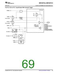
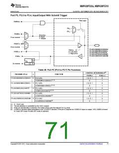
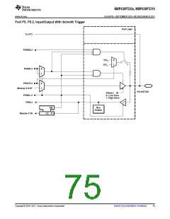
Port P3, P3.0 to P3.4, Input/Output With Schmitt Trigger
Pad Logic
P3REN.x
DVSS
DVCC
0
1
1
P3DIR.x
0
1
Direction
0: Input
1: Output
From module
P3OUT.x
0
1
From module
P3.0/UCB0SIMO/UCB0SDA
P3.1/UCB0SOMI/UCB0SCL
P3.2/UCB0CLK/UCA0STE
P3.3/UCA0TXD/UCA0SIMO
P3.4/UCA0RXD/UCA0SOMI
P3DS.x
0: Low drive
1: High drive
P3SEL.x
P3IN.x
EN
D
To module
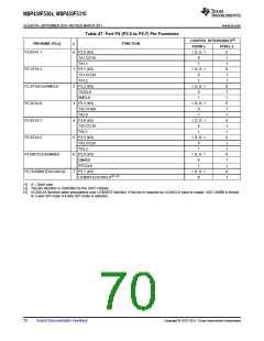
Table 48. Port P3 (P3.0 to P3.7) Pin Functions
CONTROL BITS/SIGNALS(1)
PIN NAME (P3.x)
x
FUNCTION
P3DIR.x
P3SEL.x
P3.0/UCB0SIMO/UCB0SDA
0
1
2
3
4
P3.0 (I/O)
UCB0SIMO/UCB0SDA(2) (3)
I: 0; O: 1
0
1
0
1
0
1
0
1
0
1
X
P3.1/UCB0SOMI/UCB0SCL
P3.2/UCB0CLK/UCA0STE
P3.3/UCA0TXD/UCA0SIMO
P3.4/UCA0RXD/UCA0SOMI
P3.1 (I/O)
I: 0; O: 1
UCB0SOMI/UCB0SCL(2) (3)
P3.2 (I/O)
UCB0CLK/UCA0STE(2) (4)
X
I: 0; O: 1
X
I: 0; O: 1
X
P3.3 (I/O)
UCA0TXD/UCA0SIMO(2)
P3.4 (I/O)
UCA0RXD/UCA0SOMI(2)
I: 0; O: 1
X
(1) X = Don't care
(2) The pin direction is controlled by the USCI module.
(3) If the I2C functionality is selected, the output drives only the logical 0 to VSS level.
(4) UCB0CLK function takes precedence over UCA0STE function. If the pin is required as UCB0CLK input or output, USCI A0/B0 is forced
to 3-wire SPI mode if 4-wire SPI mode is selected.
Copyright © 2010–2011, Texas Instruments Incorporated
Submit Documentation Feedback
71

 TI [ TEXAS INSTRUMENTS ]