MSP430F530x, MSP430F5310
www.ti.com
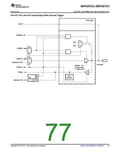
SLAS677B –SEPTEMBER 2010–REVISED MARCH 2011
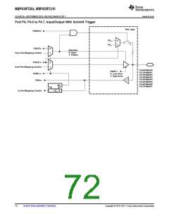
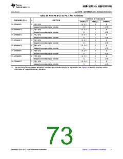
Table 49. Port P4 (P4.0 to P4.7) Pin Functions
CONTROL BITS/SIGNALS
PIN NAME (P4.x)
x
FUNCTION
P4DIR.x(1)
P4SEL.x
P4MAPx
P4.0/P4MAP0
P4.1/P4MAP1
P4.2/P4MAP2
P4.3/P4MAP3
P4.4/P4MAP4
P4.5/P4MAP5
P4.6/P4MAP6
P4.7/P4MAP7
0
P4.0 (I/O)
I: 0; O: 1
0
1
0
1
0
1
0
1
0
1
0
1
0
1
0
1
X
≤ 30
X
Mapped secondary digital function
P4.1 (I/O)
X
1
2
3
4
5
6
7
I: 0; O: 1
Mapped secondary digital function
P4.2 (I/O)
X
≤ 30
X
I: 0; O: 1
Mapped secondary digital function
P4.3 (I/O)
X
≤ 30
X
I: 0; O: 1
Mapped secondary digital function
P4.4 (I/O)
X
≤ 30
X
I: 0; O: 1
Mapped secondary digital function
P4.5 (I/O)
X
≤ 30
X
I: 0; O: 1
Mapped secondary digital function
P4.6 (I/O)
X
I: 0; O: 1
X
≤ 30
X
Mapped secondary digital function
P4.7 (I/O)
≤ 30
X
I: 0; O: 1
X
Mapped secondary digital function
≤ 30
(1) The direction of some mapped secondary functions are controlled directly by the module. See Table 9 for specific direction control
information of mapped secondary functions.
Copyright © 2010–2011, Texas Instruments Incorporated
Submit Documentation Feedback
73

 TI [ TEXAS INSTRUMENTS ]