MSP430F530x, MSP430F5310
SLAS677B –SEPTEMBER 2010–REVISED MARCH 2011
www.ti.com
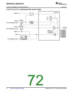
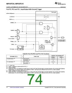
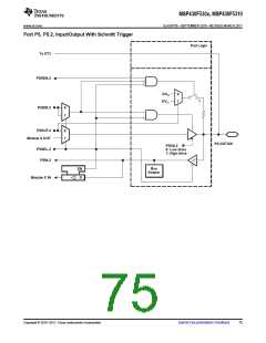
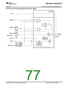
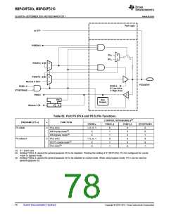
Port P5, P5.0 and P5.1, Input/Output With Schmitt Trigger
Pad Logic
to/from Reference
to ADC10
INCHx = x
P5REN.x
DVSS
DVCC
0
1
1
P5DIR.x
0
1
P5OUT.x
0
1
From module
P5.0/(A8/VeREF+)
P5.1/(A9/VeREF–)
P5DS.x
0: Low drive
1: High drive
P5SEL.x
P5IN.x
Bus
Keeper
EN
D
To module
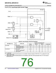
Table 50. Port P5 (P5.0 and P5.1) Pin Functions
CONTROL BITS/SIGNALS(1)
PIN NAME (P5.x)
x
FUNCTION
P5DIR.x
I: 0; O: 1
X
P5SEL.x
P5.0/A8/VeREF+(2)
0
P5.0 (I/O)(3)
A8/VeREF+(4)
P5.1 (I/O)(3)
A9/VeREF–(6)
0
1
0
1
P5.1/A9/VeREF–(5)
1
I: 0; O: 1
X
(1) X = Don't care
(2) VeREF+ available on devices with ADC10_A.
(3) Default condition
(4) Setting the P5SEL.0 bit disables the output driver as well as the input Schmitt trigger to prevent parasitic cross currents when applying
analog signals. An external voltage can be applied to VeREF+ and used as the reference for the ADC10_A when available.
(5) VeREF- available on devices with ADC10_A.
(6) Setting the P5SEL.1 bit disables the output driver as well as the input Schmitt trigger to prevent parasitic cross currents when applying
analog signals. An external voltage can be applied to VeREF- and used as the reference for the ADC10_A when available.
74
Submit Documentation Feedback
Copyright © 2010–2011, Texas Instruments Incorporated

 TI [ TEXAS INSTRUMENTS ]