MSP430F530x, MSP430F5310
www.ti.com
SLAS677B –SEPTEMBER 2010–REVISED MARCH 2011
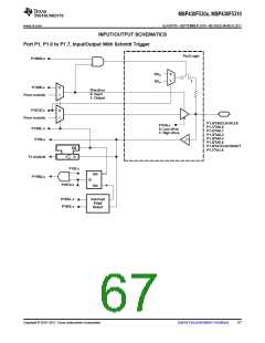
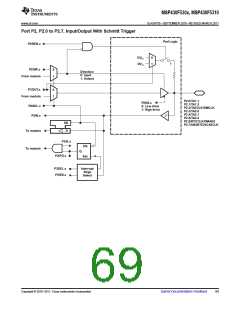
INPUT/OUTPUT SCHEMATICS
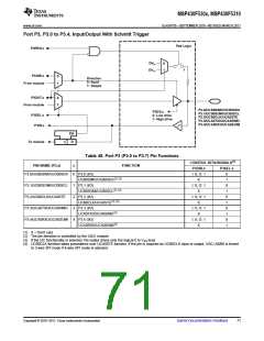
Port P1, P1.0 to P1.7, Input/Output With Schmitt Trigger
Pad Logic
P1REN.x
DVSS
DVCC
0
1
1
P1DIR.x
0
1
Direction
0: Input
1: Output
From module
P1OUT.x
0
1
From module
P1.0/TA0CLK/ACLK
P1.1/TA0.0
P1.2/TA0.1
P1.3/TA0.2
P1.4/TA0.3
P1DS.x
0: Low drive
1: High drive
P1SEL.x
P1IN.x
P1.5/TA0.4
P1.6/TA1CLK/CBOUT
P1.7/TA1.0
EN
D
To module
P1IRQ.x
P1IE.x
EN
Q
P1IFG.x
Set
P1SEL.x
P1IES.x
Interrupt
Edge
Select
Copyright © 2010–2011, Texas Instruments Incorporated
Submit Documentation Feedback
67

 TI [ TEXAS INSTRUMENTS ]