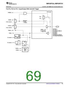
MSP430F530x, MSP430F5310
www.ti.com
SLAS677B –SEPTEMBER 2010–REVISED MARCH 2011
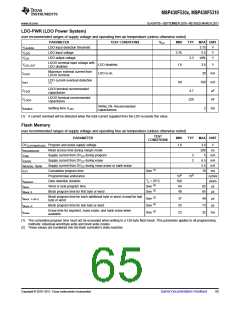
LDO-PWR (LDO Power System)
over recommended ranges of supply voltage and operating free-air temperature (unless otherwise noted)
PARAMETER
TEST CONDITIONS
VCC
MIN
TYP
MAX UNIT
VLAUNCH
VLDOI
LDO input detection threshold
LDO input voltage
3.75
5.5
V
V
V
3.76
VLDO
LDO output voltage
3.3
±9%
LDOO terminal input voltage with
LDO disabled.
VLDO_EXT
ILDOO
LDO disabled.
1.8
60
3.6
20
V
Maximum external current from
LDOO terminal.
LDO is on.
mA
mA
µF
nF
LDO current overload detection
IDET
100
(1)
LDOI terminal recommended
capacitance
CLDOI
4.7
LDOO terminal recommended
capacitance
CLDOO
tENABLE
220
Within 2%. Recommended
capacitances.
Settling time VLDO
.
2
ms
(1) A current overload will be detected when the total current supplied from the LDO exceeds this value.
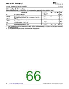
Flash Memory
over recommended ranges of supply voltage and operating free-air temperature (unless otherwise noted)
TEST
CONDITIONS
PARAMETER
MIN
TYP
MAX UNIT
DVCC(PGM/ERASE) Program and erase supply voltage
1.8
3.6
200
5
V
ns
tREADMARGIN
IPGM
Read access time during margin mode
Supply current from DVCC during program
Supply current from DVCC during erase
Supply current from DVCC during mass erase or bank erase
Cumulative program time
3
2
mA
mA
mA
ms
IERASE
6.5
2.5
16
IMERASE, IBANK
tCPT
(1)
See
Program/erase endurance
104
100
64
105
cycles
years
µs
tRetention
tWord
Data retention duration
TJ = 25°C
(2)
Word or byte program time
See
85
65
(2)
tBlock, 0
Block program time for first byte or word
See
49
µs
Block program time for each additional byte or word, except for last
byte or word
(2)
tBlock, 1–(N–1)
tBlock, N
See
37
55
23
49
73
32
µs
µs
(2)
Block program time for last byte or word
See
Erase time for segment, mass erase, and bank erase when
available.
(2)
tErase
See
ms
(1) The cumulative program time must not be exceeded when writing to a 128-byte flash block. This parameter applies to all programming
methods: individual word/byte write and block write modes.
(2) These values are hardwired into the flash controller's state machine.
Copyright © 2010–2011, Texas Instruments Incorporated
Submit Documentation Feedback
65

 TI [ TEXAS INSTRUMENTS ]