MSP430F530x, MSP430F5310
SLAS677B –SEPTEMBER 2010–REVISED MARCH 2011
www.ti.com
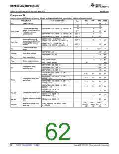
Comparator B
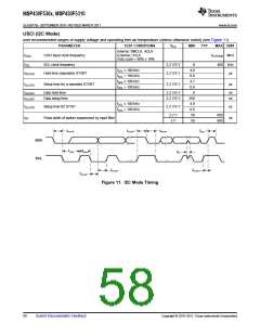
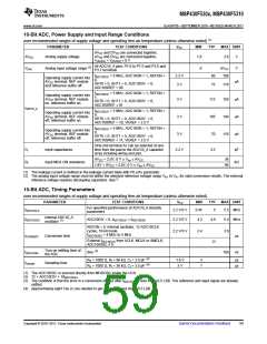
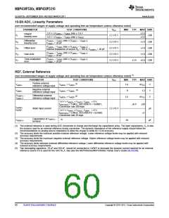
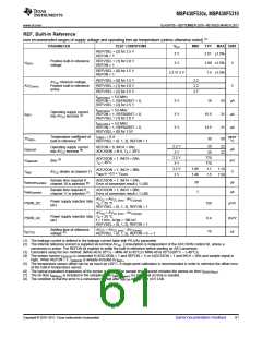
over recommended ranges of supply voltage and operating free-air temperature (unless otherwise noted)
PARAMETER
TEST CONDITIONS
VCC
MIN
TYP
MAX UNIT
VCC
Supply voltage
1.8
3.6
40
50
65
17
0.5
V
1.8 V
2.2 V
Comparator operating
supply current into AVCC
Excludes reference
resistor ladder.
CBPWRMD = 00, CBON = 1, CBRSx = 00
30
40
.
IAVCC_COMP
3 V
µA
CBPWRMD = 01, CBON = 1, CBRSx = 00
CBPWRMD = 10, CBON = 1, CBRSx = 00
2.2/3 V
2.2/3 V
10
0.1
CBREFACC = 0, CBREFLx = 01,
CBRSx = 10, REFON = 0, CBON = 0
Quiescent current of
2.2/3 V
2.2/3 V
10
17
22
µA
µA
V
resistor ladder into AVCC
Including REF module
current.
.
IAVCC_REF
CBREFACC = 1, CBREFLx = 01,
CBRSx = 10, REFON = 0, CBON = 0
Common mode input
range
VIC
VOFFSET
CIN
0
VCC-1
CBPWRMD = 00
±20
±10
mV
mV
pF
kΩ
MΩ
ns
Input offset voltage
Input capacitance
CBPWRMD = 01, 10
5
3
ON - switch closed
4
RSIN
Series input resistance
OFF - switch opened
50
CBPWRMD = 00, CBF = 0
CBPWRMD = 01, CBF = 0
CBPWRMD = 10, CBF = 0
450
600
50
Propagation delay,
response time
tPD
ns
µs
CBPWRMD = 00, CBON = 1, CBF = 1,
CBFDLY = 00
0.35
0.6
1.0
1.8
0.6
1.0
1.8
3.4
1
1.0
1.8
3.4
6.5
2
µs
µs
µs
µs
µs
µs
µs
CBPWRMD = 00, CBON = 1, CBF = 1,
CBFDLY = 01
Propagation delay with
filter active
tPD,filter
CBPWRMD = 00, CBON = 1, CBF = 1,
CBFDLY = 10
CBPWRMD = 00, CBON = 1, CBF = 1,
CBFDLY = 11
CBON = 0 to CBON = 1
CBPWRMD = 00, 01
tEN_CMP
Comparator enable time
CBON = 0 to CBON = 1
CBPWRMD = 10
1.5
Resistor reference enable
time
tEN_REF
CBON = 0 to CBON = 1
1
1.5
VIN ×
(n+0.5)
/32
VIN ×
(n+1) (n+1.5)
/32 /32
VIN ×
Reference voltage for a
given tap
VIN = reference into resistor ladder.
n = 0 to 31
VCB_REF
V
62
Submit Documentation Feedback
Copyright © 2010–2011, Texas Instruments Incorporated

 TI [ TEXAS INSTRUMENTS ]