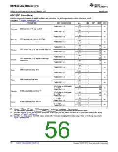
MSP430F530x, MSP430F5310
SLAS677B –SEPTEMBER 2010–REVISED MARCH 2011
www.ti.com
MAX UNIT
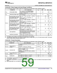
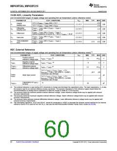
10-Bit ADC, Linearity Parameters
over recommended ranges of supply voltage and operating free-air temperature (unless otherwise noted)
PARAMETER
TEST CONDITIONS
1.4 V ≤ (VeREF+ – VeREF–)min ≤ 1.6 V
1.6 V < (VeREF+ – VeREF–)min ≤ VAVCC
VCC
MIN
TYP
±1.0
LSB
±1.0
Integral
linearity error
EI
2.2 V/3 V
Differential
linearity error
(VeREF+ – VeREF–)min ≤ (VeREF+ – VeREF–),
CVREF+ = 20 pF
ED
EO
EG
ET
2.2 V/3 V
2.2 V/3 V
2.2 V/3 V
2.2 V/3 V
±1.0 LSB
±1.0 LSB
±1.0 LSB
±2.0 LSB
(VeREF+ – VeREF–)min ≤ (VeREF+ – VeREF–),
Internal impedance of source RS < 100 Ω, CVeREF+ = 20 pF
Offset error
Gain error
(VeREF+ – VeREF–)min ≤ (VeREF+ – VeREF–),
CVREF+ = 20 pF
Total unadjusted
error
(VeREF+ – VeREF–)min ≤ (VeREF+ – VeREF–),
CVREF+ = 20 pF
±1.0
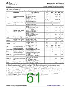
REF, External Reference
over recommended ranges of supply voltage and operating free-air temperature (unless otherwise noted)
(1)
PARAMETER
TEST CONDITIONS
VCC
MIN
TYP
MAX UNIT
Positive external
reference voltage input
(2)
VeREF+
V
V
V
eREF+ > VeREF–
1.4
AVCC
1.2
V
V
V
Negative external
reference voltage input
(3)
VeREF–
eREF+ > VeREF–
0
(VeREF+
–
Differential external
reference voltage input
(4)
eREF+ > VeREF–
1.4
AVCC
VeREF–
)
1.4 V ≤ VeREF+ ≤ VAVCC, VeREF– = 0 V,
fADC10CLK = 5 MHz, ADC10SHTx = 0x0001,
Conversion rate 200 ksps
±8.5
±26
±1
IVeREF+
IVeREF–
Static input current
2.2 V/3 V
µA
1.4 V ≤ VeREF+ ≤ VAVCC, VeREF– = 0 V,
fADC10CLK = 5 MHZ, ADC10SHTX = 0x1000,
Conversion rate 20 ksps
Capacitance at VeREF+/-
terminal
(5)
CVREF+/-
10
µF
(1) The external reference is used during ADC conversion to charge and discharge the capacitance array. The input capacitance, CI, is also
the dynamic load for an external reference during conversion. The dynamic impedance of the reference supply should follow the
recommendations on analog-source impedance to allow the charge to settle for 12-bit accuracy.
(2) The accuracy limits the minimum positive external reference voltage. Lower reference voltage levels may be applied with reduced
accuracy requirements.
(3) The accuracy limits the maximum negative external reference voltage. Higher reference voltage levels may be applied with reduced
accuracy requirements.
(4) The accuracy limits minimum external differential reference voltage. Lower differential reference voltage levels may be applied with
reduced accuracy requirements.
(5) Two decoupling capacitors, 10 µF and 100 nF, should be connected to VeREF to decouple the dynamic current required for an external
reference source if it is used for the ADC10_A. See also the MSP430x5xx/MSP430x6xx Family User's Guide (SLAU208).
60
Submit Documentation Feedback
Copyright © 2010–2011, Texas Instruments Incorporated

 TI [ TEXAS INSTRUMENTS ]