MSP430F530x, MSP430F5310
www.ti.com
SLAS677B –SEPTEMBER 2010–REVISED MARCH 2011
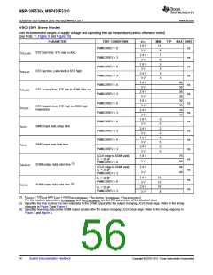
10-Bit ADC, Power Supply and Input Range Conditions
over recommended ranges of supply voltage and operating free-air temperature (unless otherwise noted)
(1)
PARAMETER
TEST CONDITIONS
VCC
MIN
TYP
MAX UNIT
AVCC and DVCC are connected together,
AVSS and DVSS are connected together,
V(AVSS) = V(DVSS) = 0 V
AVCC
V(Ax)
Analog supply voltage
1.8
3.6
V
V
All ADC10_A pins: P1.0 to P1.5 and P3.6 and
P3.7 terminals
(2)
Analog input voltage range
0
AVCC
100
fADC10CLK = 5 MHz, ADC10ON = 1, REFON =
0,
SHT0 = 0, SHT1 = 0, ADC10DIV = 0,
ADC10SREF = 00
2.2 V
3 V
60
75
Operating supply current into
AVCC terminal. REF module
and reference buffer off.
µA
µA
µA
µA
110
fADC10CLK = 5 MHz, ADC10ON = 1, REFON =
1,
SHT0 = 0, SHT1 = 0, ADC10DIV = 0,
ADC10SREF = 01
Operating supply current into
AVCC terminal. REF module
on, reference buffer on.
3 V
3 V
113
105
150
IADC10_A
fADC10CLK = 5 MHz, ADC10ON = 1, REFON =
0,
SHT0 = 0, SHT1 = 0, ADC10DIV = 0,
ADC10SREF = 10, VEREF = 2.5 V
Operating supply current into
AVCC terminal. REF module
off, reference buffer on.
140
110
fADC10CLK = 5 MHz, ADC10ON = 1, REFON =
0,
SHT0 = 0, SHT1 = 0, ADC10DIV = 0,
ADC10SREF = 11, VEREF = 2.5 V
Operating supply current into
AVCC terminal. REF module
off, reference buffer off.
3 V
70
Only one terminal Ax can be selected at one
time from the pad to the ADC10_A capacitor
array including wiring and pad.
CI
RI
Input capacitance
2.2 V
3.5
pF
AVCC > 2.0V, 0 V ≤ VAx ≤ AVCC
36
96
Input MUX ON resistance
kΩ
1.8V < AVCC < 2.0V, 0 V ≤ VAx ≤ AVCC
(1) The leakage current is defined in the leakage current table with P6.x/Ax parameter.
(2) The analog input voltage range must be within the selected reference voltage range VR+ to VR– for valid conversion results. The external
reference voltage requires decoupling capacitors. See ()
.
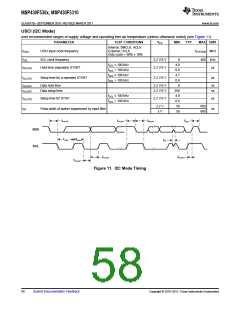
10-Bit ADC, Timing Parameters
over recommended ranges of supply voltage and operating free-air temperature (unless otherwise noted)
PARAMETER
TEST CONDITIONS
VCC
MIN
TYP
MAX UNIT
For specified performance of ADC10_A linearity
parameters
fADC10CLK
fADC10OSC
2.2 V/3 V
0.45
5
5.5 MHz
Internal ADC10_A
oscillator
ADC10DIV = 0, fADC10CLK = fADC10OSC
2.2 V/3 V
2.2 V/3 V
4.2
2.4
4.8
5.4 MHz
(1)
REFON = 0, Internal oscillator, 12 ADC10CLK
cycles, 10-bit mode
3.0
fADC10OSC = 4 MHz to 5 MHz
tCONVERT
Conversion time
µs
External fADC10CLK from ACLK, MCLK or SMCLK,
(2)
ADC10SSEL ≠ 0
Turn on settling time of
the ADC
(3)
tADC10ON
tSample
See
100
ns
(4)
RS = 1000 Ω, RI = 96 kΩ, CI = 3.5 pF
1.8 V
3 V
3
1
µs
µs
Sampling time
(4)
RS = 1000 Ω, RI = 36 kΩ, CI = 3.5 pF
(1) The ADC10OSC is sourced directly from MODOSC inside the UCS.
(2) 12 × ADC10DIV × 1/fADC10CLK
(3) The condition is that the error in a conversion started after tADC10ON is less than ±0.5 LSB. The reference and input signal are already
settled.
(4) Approximately eight Tau (τ) are needed to get an error of less than ±0.5 LSB
Copyright © 2010–2011, Texas Instruments Incorporated
Submit Documentation Feedback
59

 TI [ TEXAS INSTRUMENTS ]