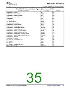
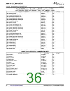
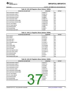
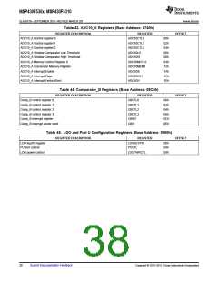
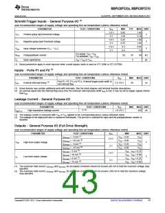
MSP430F530x, MSP430F5310
www.ti.com
SLAS677B –SEPTEMBER 2010–REVISED MARCH 2011
(1)
Absolute Maximum Ratings
over operating free-air temperature range (unless otherwise noted)
Voltage applied at VCC to VSS
–0.3 V to 4.1 V
–0.3 V to VCC + 0.3 V
±2 mA
(2)
Voltage applied to any pin (excluding VCORE, LDOI)
Diode current at any device pin
(3)
Storage temperature range, Tstg
–55°C to 150°C
95°C
Maximum junction temperature, TJ
(1) Stresses beyond those listed under "absolute maximum ratings" may cause permanent damage to the device. These are stress ratings
only, and functional operation of the device at these or any other conditions beyond those indicated under "recommended operating
conditions" is not implied. Exposure to absolute-maximum-rated conditions for extended periods may affect device reliability.
(2) All voltages referenced to VSS. VCORE is for internal device use only. No external DC loading or voltage should be applied.
(3) Higher temperature may be applied during board soldering according to the current JEDEC J-STD-020 specification with peak reflow
temperatures not higher than classified on the device label on the shipping boxes or reels.
(1)
Thermal Packaging Characteristics
PARAMETER
VALUE
30
UNIT
VQFN (RGC)
VQFN (RGZ)
LQFP (PT)
28.6
62.8
55.5
15.6
14.4
18.2
21.2
1.6
(2)
θJA
Junction-to-ambient thermal resistance, still air
°C/W
BGA (ZQE)
VQFN (RGC)
VQFN (RGZ)
LQFP (PT)
(3)
θJC(TOP)
θJC(BOTTOM)
θJB
Junction-to-case (top) thermal resistance
°C/W
°C/W
°C/W
BGA (ZQE)
VQFN (RGC)
VQFN (RGZ)
LQFP (PT)
1.6
(4)
Junction-to-case (bottom) thermal resistance
N/A
N/A
8.9
BGA (ZQE)
VQFN (RGC)
VQFN (RGZ)
LQFP (PT)
5.5
(5)
Junction-to-board thermal resistance
28.3
19.3
BGA (ZQE)
(1) N/A = not applicable
(2) The junction-to-ambient thermal resistance under natural convection is obtained in a simulation on a JEDEC-standard, High-K board, as
specified in JESD51-7, in an environment described in JESD51-2a.
(3) The junction-to-case(top) thermal resistance is obtained by simulating a cold plate test on the package top. No specific JEDEC-standard
test exists, but a close description can be found in the ANSI SEMI standard G30-88.
(4) The junction-to-case(bottom) thermal resistance is obtained by simulating a cold plate test on the exposed (power) pad. No specific
JEDEC standard test exists, but a close description can be found in the ANSI SEMI standard G30-88.
(5) The junction-to-board thermal resistance is obtained by simulating in an environment with a ring cold plate fixture to control the PCB
temperature, as described in JESD51-8.
Copyright © 2010–2011, Texas Instruments Incorporated
Submit Documentation Feedback
39

 TI [ TEXAS INSTRUMENTS ]