MSP430F530x, MSP430F5310
SLAS677B –SEPTEMBER 2010–REVISED MARCH 2011
www.ti.com
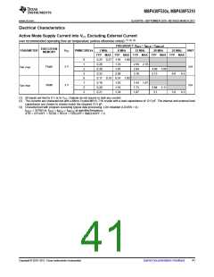
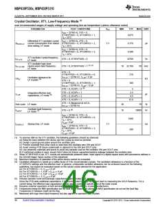
Low-Power Mode Supply Currents (Into VCC) Excluding External Current
over recommended ranges of supply voltage and operating free-air temperature (unless otherwise noted)
(1) (2)
-40°C
TYP MAX
25°C
TYP MAX
77 85
60°C
TYP MAX
80
85°C
TYP MAX
80
PARAMETER
VCC
PMMCOREVx
UNIT
2.2 V
3 V
0
3
0
3
0
1
2
0
1
2
3
0
1
2
3
0
1
2
3
73
79
97
105
11
(3) (4)
(5) (4)
Low-power mode 0
Low-power mode 2
µA
µA
LPM0,1MHz
83
6.5
92
8
88
7.5
7.9
2.6
2.7
2.9
2.8
2.9
3.0
3.1
1.9
2.0
2.1
2.2
1.8
2.0
2.1
2.2
0.26
95
8
2.2 V
3 V
6.5
7.0
1.60
1.65
1.75
1.8
1.9
2.0
2.0
1.1
1.1
1.2
1.3
0.9
1.1
1.2
1.3
0.15
ILPM2
7.0
9
8.9
3.4
3.6
3.8
3.6
3.8
4.0
4.0
2.7
2.8
2.9
3.0
2.5
2.6
2.7
2.8
0.45
13
1.90
2.00
2.15
2.1
2.2 V
Low-power mode 3,
crystal mode
ILPM3,XT1LF
2.6
6.0
µA
µA
(6) (4)
2.3
3 V
2.4
2.5
3.0
1.8
6.5
5.0
1.3
1.4
Low-power mode 3,
VLO mode(7)(4)
ILPM3,VLO
3 V
1.5
1.5
2.0
1.5
5.5
4.8
1.1
1.2
ILPM4
Low-power mode 4(8)(4)
Low-power mode 4.5(9)
3 V
3 V
µA
µA
1.2
1.3
1.6
5.0
0.8
ILPM4.5
0.18
0.35
(1) All inputs are tied to 0 V or to VCC. Outputs do not source or sink any current.
(2) The currents are characterized with a Micro Crystal MS1V-T1K crystal with a load capacitance of 12.5 pF. The internal and external load
capacitance are chosen to closely match the required 12.5 pF.
(3) Current for watchdog timer clocked by SMCLK included. ACLK = low frequency crystal operation (XTS = 0, XT1DRIVEx = 0).
CPUOFF = 1, SCG0 = 0, SCG1 = 0, OSCOFF = 0 (LPM0); fACLK = 32768 Hz, fMCLK = 0 MHz, fSMCLK = fDCO = 1 MHz
LDO disabled (LDOEN = 0).
(4) Current for brownout, high side supervisor (SVSH) normal mode included. Low side supervisor and monitors disabled (SVSL, SVML).
High side monitor disabled (SVMH). RAM retention enabled.
(5) Current for watchdog timer and RTC clocked by ACLK included. ACLK = low frequency crystal operation (XTS = 0, XT1DRIVEx = 0).
CPUOFF = 1, SCG0 = 0, SCG1 = 1, OSCOFF = 0 (LPM2); fACLK = 32768 Hz, fMCLK = 0 MHz, fSMCLK = fDCO = 0 MHz; DCO setting = 1
MHz operation, DCO bias generator enabled.
LDO disabled (LDOEN = 0)
(6) Current for watchdog timer and RTC clocked by ACLK included. ACLK = low frequency crystal operation (XTS = 0, XT1DRIVEx = 0).
CPUOFF = 1, SCG0 = 1, SCG1 = 1, OSCOFF = 0 (LPM3); fACLK = 32768 Hz, fMCLK = fSMCLK = fDCO = 0 MHz
LDO disabled (LDOEN = 0)
(7) Current for watchdog timer and RTC clocked by ACLK included. ACLK = VLO.
CPUOFF = 1, SCG0 = 1, SCG1 = 1, OSCOFF = 0 (LPM3); fACLK = fVLO, fMCLK = fSMCLK = fDCO = 0 MHz
LDO disabled (LDOEN = 0)
(8) CPUOFF = 1, SCG0 = 1, SCG1 = 1, OSCOFF = 1 (LPM4); fDCO = fACLK = fMCLK = fSMCLK = 0 MHz
LDO disabled (LDOEN = 0)
(9) Internal regulator disabled. No data retention.
CPUOFF = 1, SCG0 = 1, SCG1 = 1, OSCOFF = 1, PMMREGOFF = 1 (LPM4.5); fDCO = fACLK = fMCLK = fSMCLK = 0 MHz
42
Submit Documentation Feedback
Copyright © 2010–2011, Texas Instruments Incorporated

 TI [ TEXAS INSTRUMENTS ]