MSP430F530x, MSP430F5310
SLAS677B –SEPTEMBER 2010–REVISED MARCH 2011
www.ti.com
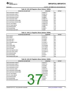
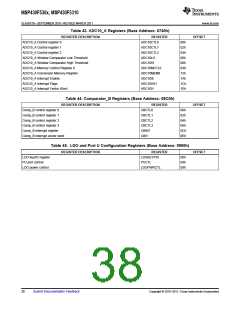
Table 43. ADC10_A Registers (Base Address: 0740h)
REGISTER DESCRIPTION
REGISTER
ADC10CTL0
OFFSET
ADC10_A Control register 0
ADC10_A Control register 1
ADC10_A Control register 2
00h
02h
04h
06h
08h
0Ah
12h
1Ah
1Ch
1Eh
ADC10CTL1
ADC10CTL2
ADC10LO
ADC10_A Window Comparator Low Threshold
ADC10_A Window Comparator High Threshold
ADC10_A Memory Control Register 0
ADC10_A Conversion Memory Register
ADC10_A Interrupt Enable
ADC10HI
ADC10MCTL0
ADC10MEM0
ADC10IE
ADC10_A Interrupt Flags
ADC10IGH
ADC10IV
ADC10_A Interrupt Vector Word
Table 44. Comparator_B Registers (Base Address: 08C0h)
REGISTER DESCRIPTION
REGISTER
CBCTL0
OFFSET
Comp_B control register 0
Comp_B control register 1
Comp_B control register 2
Comp_B control register 3
Comp_B interrupt register
00h
02h
04h
06h
0Ch
0Eh
CBCTL1
CBCTL2
CBCTL3
CBINT
Comp_B interrupt vector word
CBIV
Table 45. LDO and Port U Configuration Registers (Base Address: 0900h)
REGISTER DESCRIPTION
REGISTER
LDOKEYPID
OFFSET
LDO key/ID register
PU port control
00h
04h
08h
PUCTL
LDO power control
LDOPWRCTL
38
Submit Documentation Feedback
Copyright © 2010–2011, Texas Instruments Incorporated

 TI [ TEXAS INSTRUMENTS ]