MSP430F530x, MSP430F5310
SLAS677B –SEPTEMBER 2010–REVISED MARCH 2011
www.ti.com
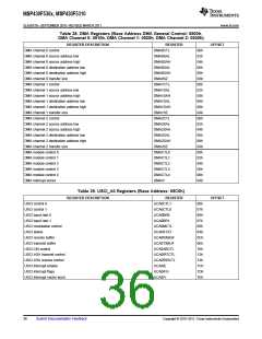
Table 38. DMA Registers (Base Address DMA General Control: 0500h,
DMA Channel 0: 0510h, DMA Channel 1: 0520h, DMA Channel 2: 0530h)
REGISTER DESCRIPTION
REGISTER
DMA0CTL
OFFSET
DMA channel 0 control
00h
02h
04h
06h
08h
0Ah
00h
02h
04h
06h
08h
0Ah
00h
02h
04h
06h
08h
0Ah
00h
02h
04h
06h
08h
0Ah
DMA channel 0 source address low
DMA channel 0 source address high
DMA channel 0 destination address low
DMA channel 0 destination address high
DMA channel 0 transfer size
DMA0SAL
DMA0SAH
DMA0DAL
DMA0DAH
DMA0SZ
DMA channel 1 control
DMA1CTL
DMA1SAL
DMA1SAH
DMA1DAL
DMA1DAH
DMA1SZ
DMA channel 1 source address low
DMA channel 1 source address high
DMA channel 1 destination address low
DMA channel 1 destination address high
DMA channel 1 transfer size
DMA channel 2 control
DMA2CTL
DMA2SAL
DMA2SAH
DMA2DAL
DMA2DAH
DMA2SZ
DMA channel 2 source address low
DMA channel 2 source address high
DMA channel 2 destination address low
DMA channel 2 destination address high
DMA channel 2 transfer size
DMA module control 0
DMACTL0
DMACTL1
DMACTL2
DMACTL3
DMACTL4
DMAIV
DMA module control 1
DMA module control 2
DMA module control 3
DMA module control 4
DMA interrupt vector
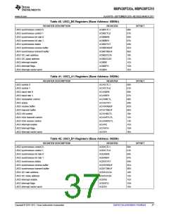
Table 39. USCI_A0 Registers (Base Address: 05C0h)
REGISTER DESCRIPTION
REGISTER
UCA0CTL1
OFFSET
USCI control 0
00h
01h
06h
07h
08h
0Ah
0Ch
0Eh
10h
12h
13h
1Ch
1Dh
1Eh
USCI control 1
UCA0CTL0
UCA0BR0
USCI baud rate 0
USCI baud rate 1
UCA0BR1
USCI modulation control
USCI status
UCA0MCTL
UCA0STAT
UCA0RXBUF
UCA0TXBUF
UCA0ABCTL
UCA0IRTCTL
UCA0IRRCTL
UCA0IE
USCI receive buffer
USCI transmit buffer
USCI LIN control
USCI IrDA transmit control
USCI IrDA receive control
USCI interrupt enable
USCI interrupt flags
USCI interrupt vector word
UCA0IFG
UCA0IV
36
Submit Documentation Feedback
Copyright © 2010–2011, Texas Instruments Incorporated

 TI [ TEXAS INSTRUMENTS ]