LM5116
SNVS499G –FEBRUARY 2007–REVISED MARCH 2013
www.ti.com
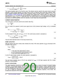
DIODE EMULATION
COMPARATOR
R
DEMB
S
SW
+
-
R
DEMB
1.215V
5V
40k
SS Latch
+
SS
-
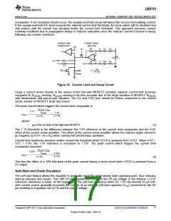
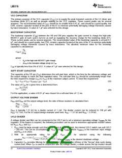
Figure 34. Diode Emulation Control
During this initial charging of CSS to the internal reference voltage, the LM5116 will force diode emulation. That
is, the low-side MOSFET will turn off for the remainder of a cycle if the sensed inductor current becomes
negative. The inductor current is sensed by monitoring the voltage between SW and DEMB. As the SS capacitor
continues to charge beyond 1.215V to 3V, the DEMB bias current will increase from 0 µA up to 40 µA. With the
use of an external DEMB resistor (RDEMB), the current sense threshold for diode emulation will increase resulting
in the gradual transition to synchronous operation. Forcing diode emulation during soft-start allows the LM5116
to start up into a pre-biased output without unnecessarily discharging the output capacitor. Full synchronous
operation is obtained if the DEMB pin is always biased to a higher potential than the SW pin when LO is high.
RDEMB = 10 kΩ will bias the DEMB pin to 0.45V minimum, which is adequate for most applications. The DEMB
bias potential should always be kept below 2V. At very light loads with larger values of output inductance and
MOSFET capacitance, the switch voltage may fall slowly. If the SW voltage does not fall below the DEMB
threshold before the end of the HO fall to LO rise dead-time, switching will default to diode emulation mode.
When RDEMB = 0Ω, the LM5116 will always run in diode emulation.
Once SS charges to 3V the SS latch is set, increasing the DEMB bias current to 65 µA. An amplifier is enabled
that regulates SS to 160 mV above the FB voltage. This feature can prevent overshoot of the output voltage in
the event the output voltage momentarily dips out of regulation. When a fault is detected (VCC under-voltage,
UVLO pin < 1.215, or EN = 0V) the soft-start capacitor is discharged. Once the fault condition is no longer
present, a new soft-start sequence begins.
HO Ouput
The LM5116 contains a high current, high-side driver and associated high voltage level shift. This gate driver
circuit works in conjunction with an external diode and bootstrap capacitor. A 1 µF ceramic capacitor, connected
with short traces between the HB pin and SW pin, is recommended. During the off-time of the high-side
MOSFET, the SW pin voltage is approximately -0.5V and the bootstrap capacitor charges from VCC through the
external bootstrap diode. When operating with a high PWM duty cycle, the buck switch will be forced off each
cycle for 450 ns to ensure that the bootstrap capacitor is recharged.
The LO and HO outputs are controlled with an adaptive deadtime methodology which insures that both outputs
are never enabled at the same time. When the controller commands HO to be enabled, the adaptive block first
disables LO and waits for the LO voltage to drop below approximately 25% of VCC. HO is then enabled after a
small delay. Similarly, when HO turns off, LO waits until the SW voltage has fallen to ½ of VCC. LO is then
enabled after a small delay. In the event that SW does not fall within approximately 150 ns, LO is asserted high.
This methodology insures adequate dead-time for appropriately sized MOSFETs.
In some applications it may be desirable to slow down the high-side MOSFET turn-on time in order to control
switching spikes. This may be accomplished by adding a resistor is series with the HO output to the high-side
gate. Values greater than 10Ω should be avoided so as not to interfere with the adaptive gate drive. Use of an
HB resistor for this function should be carefully evaluated so as not cause potentially harmful negative voltage to
the high-side driver, and is generally limited to 2.2Ω maximum.
18
Submit Documentation Feedback
Copyright © 2007–2013, Texas Instruments Incorporated
Product Folder Links: LM5116

 TI [ TEXAS INSTRUMENTS ]