LM5116
www.ti.com
SNVS499G –FEBRUARY 2007–REVISED MARCH 2013
The LM5116 oscillator has a maximum programmable frequency that is dependent on the VCC voltage. If VCC is
above 6V, the frequency can be programmed up to 1 MHz. If VCCX is used to bias VCC and VCCX < 6V, the
maximum programmable oscillator frequency is 750 kHz.
The RT/SYNC pin can be used to synchronize the internal oscillator to an external clock. The external clock must
be a higher frequency than the free-running frequency set by the RT resistor. The internal oscillator can be
synchronized to an external clock by AC coupling a positive edge into the RT/SYNC pin. The voltage at the
RT/SYNC pin is nominally 1.215V and must exceed 4V to trip the internal synchronization pulse detection. A 5V
amplitude signal and 100 pF coupling capacitor are recommended. The free-running frequency should be set
nominally 15% below the external clock. Synchronizing above twice the free-running frequency may result in
abnormal behavior of the pulse width modulator.
Error Amplifier and PWM Comparator
The internal high-gain error amplifier generates an error signal proportional to the difference between the
regulated output voltage and an internal precision reference (1.215V). The output of the error amplifier is
connected to the COMP pin allowing the user to provide loop compensation components, generally a type II
network. This network creates a pole at very low frequency, a mid-band zero, and a noise reducing high
frequency pole. The PWM comparator compares the emulated current sense signal from the RAMP generator to
the error amplifier output voltage at the COMP pin.
Ramp Generator
The ramp signal used in the pulse width modulator for current mode control is typically derived directly from the
buck switch current. This switch current corresponds to the positive slope portion of the inductor current. Using
this signal for the PWM ramp simplifies the control loop transfer function to a single pole response and provides
inherent input voltage feed-forward compensation. The disadvantage of using the buck switch current signal for
PWM control is the large leading edge spike due to circuit parasitics that must be filtered or blanked. Also, the
current measurement may introduce significant propagation delays. The filtering, blanking time and propagation
delay limit the minimal achievable pulse width. In applications where the input voltage may be relatively large in
comparison to the output voltage, controlling small pulse widths and duty cycles is necessary for regulation. The
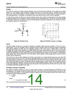
LM5116 utilizes a unique ramp generator which does not actually measure the buck switch current but rather
reconstructs the signal. Representing or emulating the inductor current provides a ramp signal to the PWM
comparator that is free of leading edge spikes and measurement or filtering delays. The current reconstruction is
comprised of two elements, a sample-and-hold DC level and an emulated current ramp.
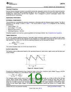
t
ON
(5 mA/V x (VIN-VOUT) + 25 mA) x
C
RAMP
RAMP
Sample and Hold
DC Level
10 x R V/A
S
t
ON
Figure 31. Composition of Current Sense Signal
The sample-and-hold DC level is derived from a measurement of the recirculating current through either the low-
side MOSFET or current sense resistor. The voltage level across the MOSFET or sense resistor is sampled and
held just prior to the onset of the next conduction interval of the buck switch. The current sensing and sample-
and-hold provide the DC level of the reconstructed current signal. The positive slope inductor current ramp is
emulated by an external capacitor connected from the RAMP pin to the AGND and an internal voltage controlled
current source. The ramp current source that emulates the inductor current is a function of the VIN and VOUT
voltages per the following equation:
IR = 5 µA/V x (VIN - VOUT) + 25 µA
(2)
Copyright © 2007–2013, Texas Instruments Incorporated
Submit Documentation Feedback
15
Product Folder Links: LM5116

 TI [ TEXAS INSTRUMENTS ]