LM26420, LM26420-Q0, LM26420-Q1
SNVS579J –FEBRUARY 2009–REVISED SEPTEMBER 2015
www.ti.com
Application Information (continued)
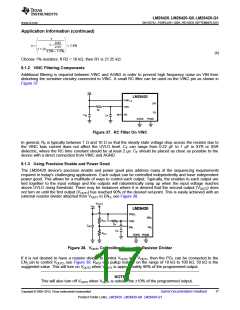
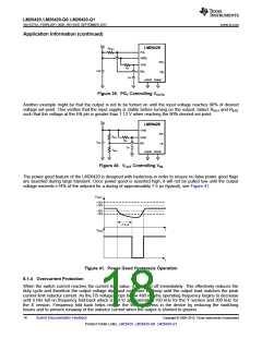
Figure 39. PG1 Controlling VOUT2
Another example might be that the output is not to be turned on until the input voltage reaches 90% of desired
voltage set-point. This verifies that the input supply is stable before turning on the output. Select REN1 and REN2
such that the voltage at the EN pin is greater than 1.12 V when reaching the 90% desired set-point.
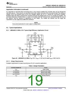
Figure 40. VOUT Controlling VIN
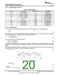
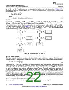
The power good feature of the LM26420 is designed with hysteresis in order to ensure no false power good flags
are asserted during large transient. Once power good is asserted high, it will not be pulled low until the output
voltage exceeds ±14% of the setpoint for a during of approximately 7.5 µs (typical), see Figure 41.
VOUT
+14%
+10%
-10%
-14%
~7.5 Ps
t
VPG
t
Figure 41. Power Good Hysteresis Operation
8.1.4 Overcurrent Protection
When the switch current reaches the current limit value, it is turned off immediately. This effectively reduces the
duty cycle and therefore the output voltage dips and continues to droop until the output load matches the peak
current limit inductor current. As the FB voltage drops below 480 mV the operating frequency begins to decrease
until it hits full on frequency fold-back which is set to approximately 150 kHz for the Y version and 300 kHz for
the X version. Frequency fold back helps reduce the thermal stress in the device by reducing the switching
losses and to prevent runaway of the inductor current when the output is shorted to ground.
18
Submit Documentation Feedback
Copyright © 2009–2015, Texas Instruments Incorporated
Product Folder Links: LM26420 LM26420-Q0 LM26420-Q1

 TI [ TEXAS INSTRUMENTS ]