LM26420, LM26420-Q0, LM26420-Q1
SNVS579J –FEBRUARY 2009–REVISED SEPTEMBER 2015
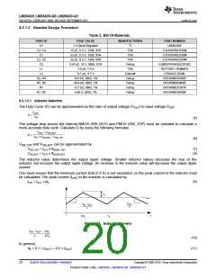
www.ti.com
8 Application and Implementation
NOTE
Information in the following applications sections is not part of the TI component
specification, and TI does not warrant its accuracy or completeness. TI’s customers are
responsible for determining suitability of components for their purposes. Customers should
validate and test their design implementation to confirm system functionality.
8.1 Application Information
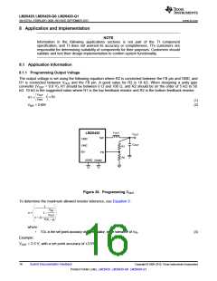
8.1.1 Programming Output Voltage
The output voltage is set using the following equation where R2 is connected between the FB pin and GND, and
R1 is connected between VOUT and the FB pin. A good value for R2 is 10 kΩ. When designing a unity gain
converter (VOUT = 0.8 V), R1 should be between 0 Ω and 100 Ω, and R2 should be on the order of 5 kΩ to 50
kΩ. 10 kΩ is the suggested value where R1 is the top feedback resistor and R2 is the bottom feedback resistor.
VOUT
x R2
- 1
R1 =
VREF
(1)
(2)
VREF = 0.80V
L
OUT
LM26420
V
OUT
SW
VIND
C
OUT
VINC
EN
R1
R2
FB
AGND
PGND
Figure 36. Programming VOUT
To determine the maximum allowed resistor tolerance, use Equation 3:
1
VFB
V =
1 ꢀ
VOUT
TOL ꢀꢁI
1 + 2x
where
•
TOL is the set point accuracy of the regulator, is the tolerance of VFB
.
(3)
Example:
VOUT = 2.5 V, with a set point accuracy of ±3.5%.
16
Submit Documentation Feedback
Copyright © 2009–2015, Texas Instruments Incorporated
Product Folder Links: LM26420 LM26420-Q0 LM26420-Q1

 TI [ TEXAS INSTRUMENTS ]