LM26420, LM26420-Q0, LM26420-Q1
www.ti.com
SNVS579J –FEBRUARY 2009–REVISED SEPTEMBER 2015
Application Information (continued)
It is important to note that when recovering from a over-current condition the converter does not go through the
soft-start process. There may be an overshoot due to the sudden removal of the overcurrent fault. The reference
voltage at the non-inverting input of the error amplifier always sits at 0.8 V during the overcurrent condition,
therefore when the fault is removed the converter bring the FB voltage back to 0.8 V as quickly as possible. The
overshoot depend on whether there is a load on the output after the removal of the overcurrent fault, the size of
the inductor, and the amount of capacitance on the output. The smaller the inductor and the larger the
capacitance on the output the smaller the overshoot.
NOTE
Overcurrent protection for each output is independent.
8.2 Typical Applications
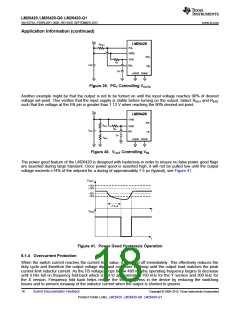
8.2.1 LM26420X 2.2-MHz, 0.8-V Typical High-Efficiency Application Circuit
Vin
3V to 5.5V
C
R
7
C
5
C
4
3
R
5
R
6
VIN
1
VIN
c
VIN
2
PG
PG
EN
SW
FB
1
2
2
2
2
LM26420
EN
1
VOUT2
0.8V/2A
VOUT1
1.8V/2A
L
L
2
1
SW
1
R
R
1
2
FB
1
C1
C
1
C
6
PGND , PGND ,
1
2
AGND, DAP
R
3
R
4
Figure 42. LM26420X (2.2 MHz): VIN = 5 V, VOUT1 = 1.8 V at 2 A and VOUT2 = 0.8 V at 2 A
8.2.1.1 Design Requirements
Example requirements for typical synchronous DC-DC converter applications:
Table 1. Design Parameters
DESIGN PARAMETER
VOUT
VALUE
Output voltage
VIN (minimum)
VIN (maximum)
IOUT (maximum)
ƒSW
Maximum input voltage
Minimum input voltage
Maximum output current
Switching frequency
Copyright © 2009–2015, Texas Instruments Incorporated
Submit Documentation Feedback
19
Product Folder Links: LM26420 LM26420-Q0 LM26420-Q1

 TI [ TEXAS INSTRUMENTS ]