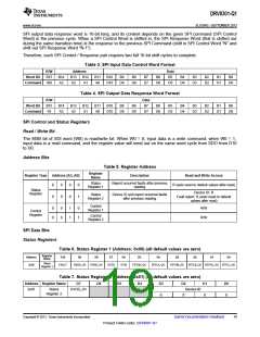
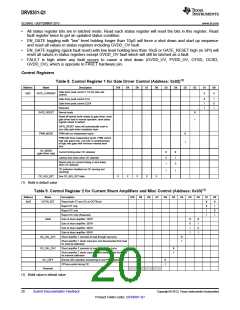
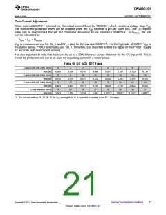
DRV8301-Q1
www.ti.com
SLOS842 –SEPTEMBER 2013
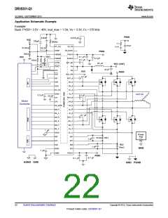
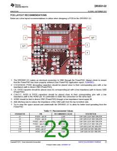
PCB LAYOUT RECOMMENDATIONS
Below are a few layout recommendations to utilize when designing a PCB for the DRV8301-Q1.
2
2
1
6/7
5
4
6/7
3
XX
1. The DRV8301-Q1 makes an electrical connection to GND through the PowerPAD. Always check to ensure
that the PowerPAD has been properly soldered (See PowerPAD application report, SLMA002).
2. C1/C2/C8/C9, PVDD decoupling capacitors should be placed close to their corresponding pins with a low
impedance path to device GND (PowerPAD).
3. C4, GVDD capacitor should be placed close its corresponding pin with a low impedance path to device GND
(PowerPAD).
4. C16/C17, AVDD & DVDD capacitors should be placed close to their corresponding pins with a low
impedance path to the AGND pin. It’s preferable to make this connection on the same layer.
5. AGND should be tied to device GND (PowerPAD) through a low impedance trace/copper fill.
6. Add stitching vias to reduce the impedance of the GND path from the top to bottom side.
7. Try to clear the space around and underneath the DRV8301-Q1 to allow for better heat spreading from the
PowerPAD.
Table 11. Recommended Values
DESIGNATOR
PIN
RECOMMENDED VALUE
DESCRIPTION
C1
C2
PVDD1 – pin 29
PVDD1 – pin 29
PVDD2 – pins 53 & 54
PVDD2 – pins 53 & 54
GVDD – pin 13
2.2uF
0.1uF
2.2uF
0.1uF
2.2uF
1.0uF
1.0uF
CAP CER 2.2UF 100V 10% X7R
CAP CER 0.1UF 100V 10% X7R
CAP CER 2.2UF 100V 10% X7R
CAP CER 0.1UF 100V 10% X7R
CAP CER 2.2UF 25V 10% X7R
CAP CER 1UF 25V 10% X7R
CAP CER 1UF 25V 10% X7R
C8
C9
C4
C16
C17
AVDD – pin 27
DVDD – pin 23
Copyright © 2013, Texas Instruments Incorporated
Submit Documentation Feedback
23
Product Folder Links: DRV8301-Q1

 TI [ TEXAS INSTRUMENTS ]