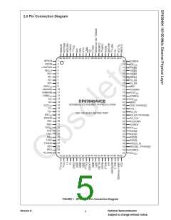
2.0 Pin Description (Continued)
2.4 CLOCK INTERFACE
Signal Name
Type
Pin #
Description
REFIN
I
86
REFERENCE INPUT: 25 MHz TTL reference clock input. This clock can be
supplied from an external oscillator module or from the CLK25M output (pin 81).
CLK25M
O, Z
81
25 MHz CLOCK OUTPUT: Derived from the 50 MHz OSCIN input. When not in
use, this clock output may be shut off through software by setting bit 7 of the PCS
Configuration Register at address 17h. This output remains unaffected by
hardware and software reset.
OSCIN
X2
I
2
OSCILLATOR INPUT: 50 MHz 50 ppm external TTL oscillator input. If not used,
pull down to GND (4.7 kΩ pull down resistor suggested).
O
34
CRYSTAL OSCILLATOR OUTPUT: External 20 MHz
0.005% crystal
connection. Used for 10BASE-T timing. When using an external 20 MHz oscillator
connected to X1 or with no reference to X1, leave this pin unconnected.
X1
I
33
CRYSTAL OSCILLATOR INPUT: External 20 MHz 0.005% crystal connection.
Used for 10BASE-T timing and Auto-Negotiation. If not used, this pin should be
pulled up to VCC. (4.7 kΩ pull up resistor suggested). When pulled high, the
DP83840A detects this condition, enables the internal 2.5 divider, and switches
the 10 Mb/s and Auto-Negotiation circuitry to the internally derived 20 MHz clock.
I = TTL/CMOS input
O = TTL/CMOS output
Z = TRI-STATE output
J = IEEE 1149.1 pin
Version A
National Semiconductor
8

 TI [ TEXAS INSTRUMENTS ]