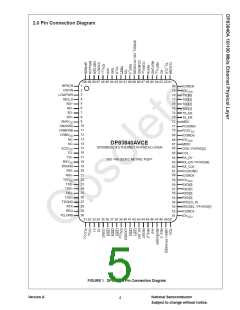
2.0 Pin Description
The DP83840A pins are classified into the following interface categories (each interface is described in the sections that
follow):
MII INTERFACE
LED INTERFACE
100 Mb/s SERIAL PMD INTERFACE
10 Mb/s INTERFACE
IEEE 1149.1 INTERFACE
PHY ADDRESS INTERFACE
MISCELLANEOUS PINS
POWER AND GROUND PINS
SPECIAL CONNECT PINS
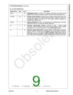
CLOCK INTERFACE
DEVICE CONFIGURATION INTERFACE
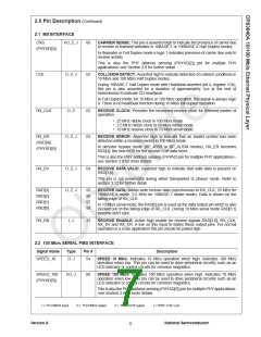
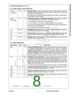
2.1 MII INTERFACE
Signal Name
Type
Pin #
Description
TX_CLK
O, Z
82
TRANSMIT CLOCK: Transmit clock output from the DP83840A:
25 MHz nibble transmit clock derived from Clock Generator Module's (CGM) PLL
in 100BASE-TX mode
2.5 MHz transmit clock in 10BASE-T nibble mode
10 MHz transmit clock in 10BASE-T serial mode
TXD[3]
TXD[2]
TXD[1]
TXD[0]
I, J
75
76
77
78
TRANSMIT DATA: Transmit data MII input pins that accept nibble data during
normal nibble-wide MII operation at either 2.5 MHz (10BASE-T mode) or 25MHz
(100BASE-X mode)
In 10 Mb/s serial mode, the TXD[0] pin is used as the serial data input pin. TXD[3:1]
are ignored.
TX_EN
I, J
I, J
74
TRANSMIT ENABLE: Active high input indicates the presence of valid nibble data
on TXD[3:0] for both 100 Mb/s or 10 Mb/s nibble mode.
In 10 Mb/s serial mode, active high indicates the presence of valid 10 Mb/s data on
TXD[0].
TX_ER
73
TRANSMIT ERROR: In 100 Mb/s mode, when this signal is high and TX_EN is
active the HALT symbol is substituted for the actual data nibble.
(TXD[4])
In 10 Mb/s mode, this input is ignored.
In encoder bypass mode (BP_4B5B or BP_ALIGN), TX_ER becomes the TXD [4]
pin, the new MSB for the transmit 5-bit data word.
MDC
I,J
72
67
MANAGEMENT DATA CLOCK: Synchronous clock to the MDIO management
data input/output serial interface which may be asynchronous to transmit and
receive clocks. The maximum clock rate is 2.5 MHz. There is no minimum clock
rate.
MDIO
I/O, Z, J
MANAGEMENT DATA I/O: Bi-directional management instruction/data signal that
may be sourced by the station management entity or the PHY. This pin requires a
1.5kΩ pullup resistor.
I = TTL/CMOS input
O = TTL/CMOS output
Z = TRI-STATE output
J = IEEE 1149.1 pin
Version A
National Semiconductor
Subject to change without notice.
5

 TI [ TEXAS INSTRUMENTS ]