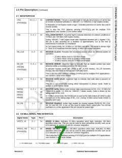
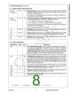
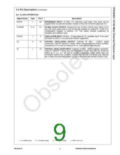
2.0 Pin Description (Continued)
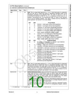
2.5 DEVICE CONFIGURATION INTERFACE
10BTSER
I, J
98
SERIAL/NIBBLE SELECT:
10 Mb/s Serial Operation:
When set high, this input selects serial data transfer mode. Transmit and receive
data is exchanged serially at a 10 MHz clock rate on the least significant bits of the
nibble-wide MII data buses, pins TXD[0] and RXD[0] respectively. This mode is
intended for use with the DP83840A connected to a device (MAC or Repeater)
using a 10 Mb/s serial interface. Serial operation is not supported in 100 Mb/s
mode, therefore this input is ignored during 100 Mb/s operation
10 and 100 Mb/s Nibble Operation:
When set low, this input selects the MII compliant nibble data transfer mode.
Transmit and receive data is exchanged in nibbles on the TXD[3:0] and RXD[3:0]
pins respectively.
At power-up/reset, the value on this pin (set by a pull-up or pull-down resistor,
typically 4.7 kΩ) is latched into bit 9 of the 10BASE-T Status Register at address
1Bh.
BPALIGN
BP4B5B
I, J
99
BYPASS ALIGNMENT: Allows 100 Mb/s transmit and receive data streams to
bypass all of the transmit and receive operations when set high. Refer to Figures 4
and 5. Note that the PCS signaling (CRS, RX_DV, RX_ER, and COL) is not
meaningful during this mode. Additionally TXD[4]/TX_ER is always active.
At power-up/reset, the value on this pin (set by a pull-up or pull-down resistor,
typically 4.7 kΩ) is latched into bit 12 of the Loopback, Bypass and Receiver Error
Mask Register at address 18h.
I, J
100
BYPASS 4B5B ENCODER/DECODER: Allows 100 Mb/s transmit and receive
data streams to bypass the 4B to 5B encoder and 5B to 4B decoder circuits when
set high. All PCS signaling (CRS, RX_DV, RX_ER, and COL) remain active and
unaffected by this bypass mode. Additionally, TXD[4]/TX_ER is gated by TX_EN.
Refer to figures 4 and 5.
At power-up/reset, the value on this pin (set by a pull-up or pull-down resistor,
typically 4.7 kΩ) is latched into bit 14 of the Loopback, Bypass and Receiver Error
Mask Register at address 18h.
BPSCR
I, J
1
BYPASS SCRAMBLER/DESCRAMBLER: Allows 100 Mb/s transmit and receive
data streams to bypass the scrambler and descrambler circuits when set high to
facilitate 100BASE-FX operation. All PCS signaling (CRS, RX_DV, RX_ER, and
COL) remain active and unaffected by this bypass mode. Refer to figures 4 and 5.
At power-up/reset, the value on this pin (set by a pull-up or pull-down resistor,
typically 4.7 kΩ) is latched into bit 13 of the Loopback, Bypass and Receiver Error
Mask Register at address 18h.
I = TTL/CMOS input
O = TTL/CMOS output
Z = TRI-STATE output
J = IEEE 1149.1 pin
Version A
National Semiconductor
10

 TI [ TEXAS INSTRUMENTS ]