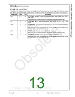
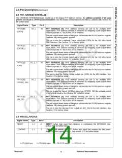
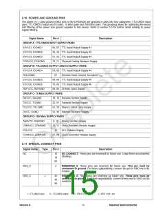
2.0 Pin Description (Continued)
2.7 IEEE 1149.1 INTERFACE
The IEEE 1149.1 Standard Test Access Port and Boundary Scan (sometimes referred to as JTAG) interface signals
allow system level boundary scan to be performed. These pins may be left floating when JTAG testing is not required.
Signal Name
Type
Pin #
Description
TDO
O, Z
50
TEST DATA OUTPUT: Serial instruction/test output data for the IEEE 1149.1
scan chain.
If Boundary-Scan is not implemented this pin may be left unconnected (NC).
TDI
I
I
91
92
TEST DATA INPUT: Serial instruction/test input data for the IEEE 1149.1 scan
chain.
TRST
TEST RESET: An asynchronous low going pulse will reset and initialize the IEEE
1149.1 test circuitry.
If Boundary-Scan is not implemented, this pin may be left unconnected (NC) since
it has an internal pull-up resistor (10 kΩ).
TCLK
TMS
I
I
93
94
TEST CLOCK: Test clock for the IEEE 1149.1 circuitry.
If Boundary-Scan is not implemented this pin may be left unconnected (NC).
TEST MODE SELECT: Control input to the IEEE 1149.1 test circuitry.
If Boundary-Scan is not implemented, this pin may be left unconnected (NC) since
it has an internal pull-up resistor (10 kΩ).
I = TTL/CMOS input
O = TTL/CMOS output
Z = TRI-STATE output
J = IEEE 1149.1 pin
Version A
National Semiconductor
12

 TI [ TEXAS INSTRUMENTS ]