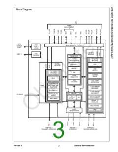
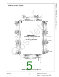
2.0 Pin Description (Continued)
2.1 MII INTERFACE
CRS
I/O, Z, J
66
65
CARRIER SENSE: This pin is asserted high to indicate the presence of carrier due
to receive or transmit activities in 10BASE-T or 100BASE-X Half Duplex modes.
(PHYAD[2])
In Repeater or Full Duplex mode a logic 1 indicates presence of carrier due only to
receive activity.
This is also the PHY address sensing (PHYAD[2]) pin for multiple PHY
applications--see Section 2.8 for further detail.
COL
O, Z, J
COLLISION DETECT: Asserted high to indicate detection of collision conditions in
10 Mb/s and 100 Mb/s Half Duplex modes.
During 10BASE-T Half Duplex mode with Heartbeat asserted (bit 4, register 1Ch),
this pin is also asserted for a duration of approximately 1µs at the end of
transmission to indicate CD heartbeat.
In Full Duplex mode, for 10 Mb/s or 100 Mb/s operation, this signal is always logic
0. There is no heartbeat function during 10 Mb/s full duplex operation.
RX_CLK
O, Z
62
63
RECEIVE CLOCK: Provides the recovered receive clock for different modes of
operation:
• 25 MHz nibble clock in 100 Mb/s mode
• 2.5 MHz nibble clock in 10 Mb/s nibble mode
• 10 MHz receive clock in 10 Mb/s serial mode
RX_ER
O, Z, J
RECEIVE ERROR: Asserted high to indicate that an invalid symbol has been
detected within a received packet in 100 Mb/s mode.
(RXD[4])
(PHYAD[4])
In decoder bypass mode (BP_4B5B or BP_ALIGN modes), RX_ER becomes
RXD[4], the new MSB for the receive 5-bit data word.
This is also the PHY address sensing (PHYAD) pin for multiple PHY applications--
see Section 2.8 for more details.
RX_DV
O, Z, J
O, Z, J
64
RECEIVE DATA VALID: Asserted high to indicate that valid data is present on
RXD[3:0].
This pin is not meaningful during either transparent or phaser mode. Refer to
section 3.12 for further detail.
RXD[3]
RXD[2]
RXD[1]
RXD[0]
55
56
57
58
RECEIVE DATA: Nibble wide receive data (synchronous to RX_CLK, 25 MHz for
100BASE-X mode, 2.5 MHz for 10BASE-T nibble mode). Data is driven on the
falling edge of RX_CLK.
In 10 Mb/s serial mode, the RXD[0] pin is used as the data output pin which is also
clocked out on the falling edge of RX_CLK. During 10 Mb/s serial mode RXD[3:1]
become don't care.
RX_EN
I, J
43
RECEIVE ENABLE: Active high enable for receive signals RXD[3:0], RX_CLK,
RX_DV and RX_ER. A low on this input tri-states these output pins. For normal
operation in a node application this pin should be pulled high.
2.2 100 Mb/s SERIAL PMD INTERFACE
Signal Name
Type
Pin #
Description
SPEED_10
O, J
54
SPEED 10 Mb/s: Indicates 10 Mb/s operation when high. Indicates 100 Mb/s
operation when low. This pin can be used to drive peripheral circuitry such as an
LED indicator or control circuits for common magnetics.
SPEED_100
(PHYAD[3])
I/O, J
89
SPEED 100 Mb/s: Indicates 100 Mb/s operation when high. Indicates 10 Mb/s
operation when low. This pin can be used to drive peripheral circuitry such as an
LED indicator or control circuits for common magnetics.
This is also the PHY address sensing (PHYAD[3]) pin for multiple PHY applications-
-see Section 2.8 for more details.
I = TTL/CMOS input
O = TTL/CMOS output
Z = TRI-STATE output
J = IEEE 1149.1 pin
Version A
National Semiconductor
6

 TI [ TEXAS INSTRUMENTS ]