2.0 Pin Description (Continued)
2.5 DEVICE CONFIGURATION INTERFACE
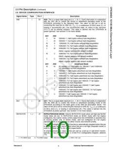
Signal Name
Type
Pin #
Description
AN0
I
95
AN0: This is a quad state input pin (i.e, 1, M, 0, Clock) that works in conjunction
with the AN1 pin to control the forced or advertised operating mode of the
DP83840A according to the following table. The value on this pin is set by
connecting the input pin to GND (0), VCC (1), a continuous 25 MHz clock (C), or
leaving it unconnected (M.) The unconnected state, M, refers to the mid-level
(VCC 2) set by internal resistors. This value is latched into the DP83840A at
power-up/reset. See section 3.9 for more details.
AN1
0
AN0
M
Forced Mode
10BASE-T, Half-Duplex without Auto-Negotiation
10BASE-T, Full Duplex without Auto-Negotiation
100BASE-TX, Half-Duplex without Auto-Negotiation
100BASE-TX, Full Duplex without Auto-Negotiation
100BASE-TX, Full Duplex without Auto-Negotiation
ANAR, register address 04h default modified
100BASE-TX, Full Duplex without Auto-Negotiation
ANAR, register address 04h default modified
100BASE-TX, Half Duplex without Auto-Negotiation
ANAR, register address 04h default modified
Advertised Mode
1
M
M
0
M
1
C
M
M
C
C
C
AN1
AN0
M
M
All capable (i.e. Full Duplex for 10BASE-T and 100BASE-
TX) advertised via Auto-Negotiation
0
0
1
1
C
0
1
0
1
1
10BASE-T, Half-Duplex advertised via Auto-Negotiation
10BASE-T, Full Duplex advertised via Auto-Negotiation
100BASE-TX, Half-Duplex advertised via Auto-Negotiation
100BASE-TX, Full Duplex advertised via Auto-Negotiation
100BASE-TX Full Duplex and 10BASE-T Full Duplex
advertised via Auto-Negotiation
C
1
0
0
C
C
100BASE-TX Half Duplex and 10BASE-T Half Duplex
advertised via Auto-Negotiation
100BASE-TX Half Duplex and 100BASE-TX Full Duplex
advertised via Auto-Negotiation
10BASE-T Half Duplex and 10BASE-T Full Duplex
advertised via Auto-Negotiation
AN1
I
46
47
AN1: This is a quad-state input pin (i.e., 1, M, 0, Clock) that works in conjunction
with the AN0 pin to control the forced or advertised operating mode of the
DP83840A according to the table given in the AN0 pin description above. The
value on this pin is set by connecting the input pin to GND (0), VCC (1), a continuous
25 MHz clock (C), or leaving it unconnected (M.) This value is latched into the
DP83840A at power-up/reset. See Section 3.9 for more details.
REPEATER
I, J
REPEATER/NODE MODE: Selects REPEATER mode when set high and NODE
mode when set low. In REPEATER mode (or NODE mode with Full Duplex
configured), the Carrier Sense (CRS) output from the DP83840A is asserted due
to receive activity only. In NODE mode, and not configured for Full Duplex
operation, CRS is asserted due to either receive and transmit activity.
The Carrier Integrity Monitor (CIM) function is automatically disabled when this pin
is set low (node mode) and enabled when this pin is set high (Repeater mode) in
order to facilitate 802.3u /D5.3 CIM requirements.
At power-up/reset, the value on this pin (set by a pull-up or pull-down resistor,
typically 4.7 kΩ) is latched to bit 12 of the PCS Configuration Register, address
17h.
I = TTL/CMOS input
O = TTL/CMOS output
Z = TRI-STATE output
J = IEEE 1149.1 pin
Version A
National Semiconductor
9

 TI [ TEXAS INSTRUMENTS ]